G4APV's EB104
Construction Page
EB104
This
web page
contains a sort running log about the construction of a MRF150 based
600W linear amp. The basis of the amp is an old but reliable
design by Motorola that came out as Engineering
Bulletin 104,
hence EB104.
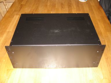
Case
The
case came from Maplin.
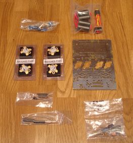
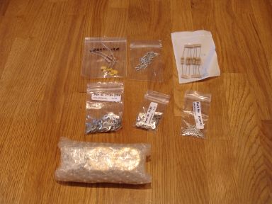
Parts
So what goes into the case? Here is the kit of EB104 parts
that I
got
from Communication
Concepts for the amplifier
itself:
Attenuator
As
well as that I needed a few other parts, these are for the
attenuator to drop 20W down to 6W. This 6dB odd loss ensures
that
most HF transceivers with a typical low power output of about 10W can
be used to drive the amplifier with a bit of a margin of safety.
It also ensures the input impedance to the amplifier is more closely
controlled. The parts came from mainly from JAB
components.
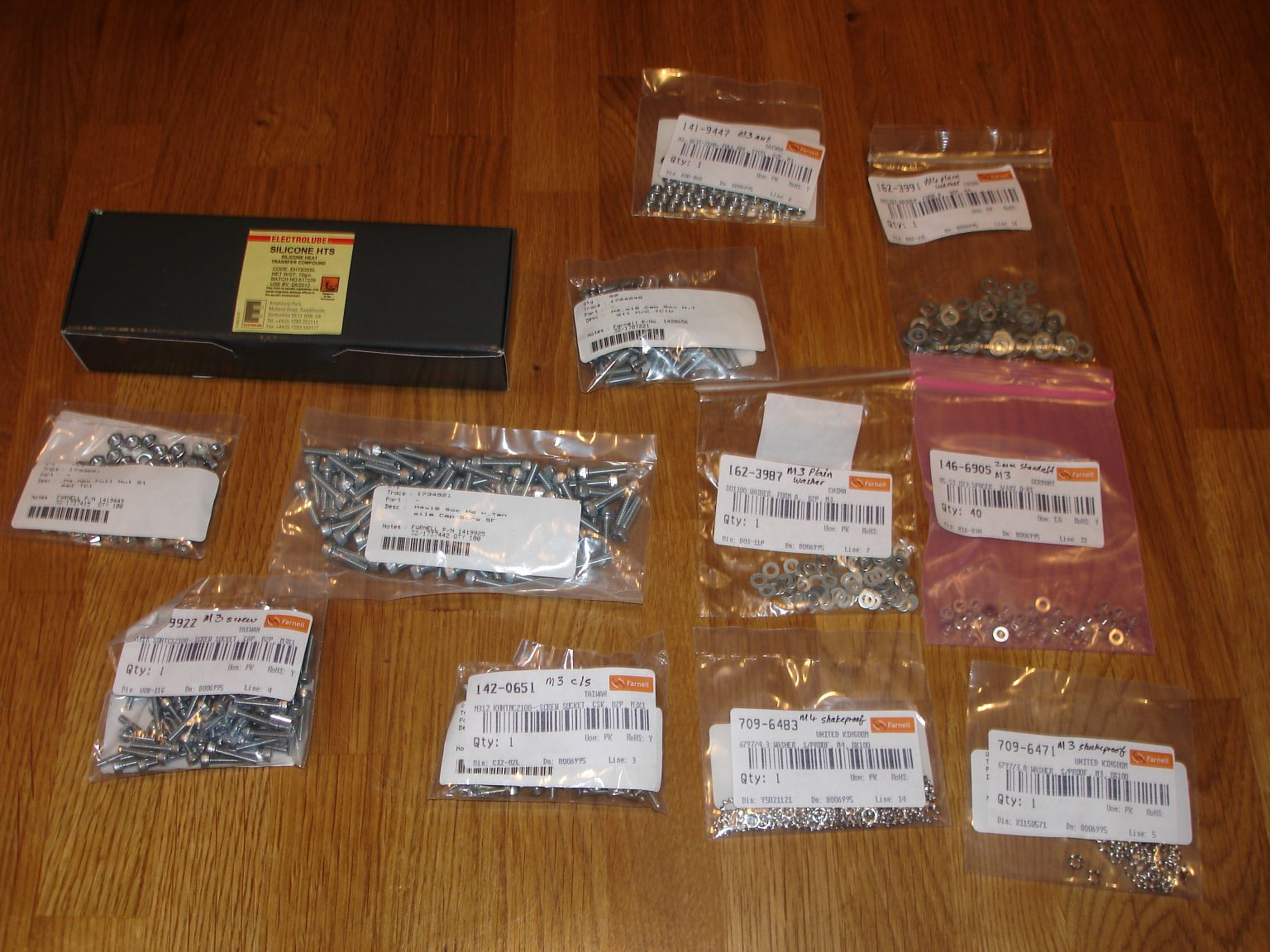
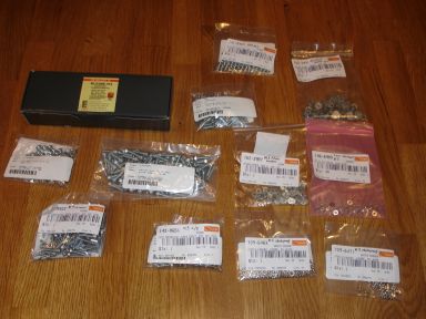
Hardware
I
quickly came to the conclusion I would need quite a few nuts, bolts and
other hardware. I used M3 and M4 nuts and bolts as they
fitted the devices.. This lot came from Farnell:
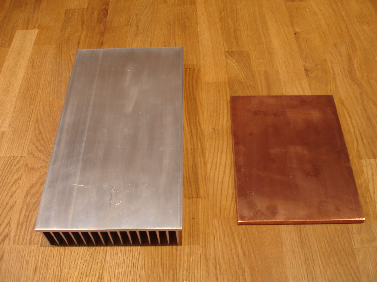
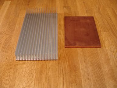
Thermal Issues
WIth 600W out and about 60% efficiency then there is as much as 400W to
get rid of. This means getting the heat away from the devices
with a copper spreader and then getting rid of it with a heatsink.
Both the
spreader and the heatsink also came from Communication Concepts:

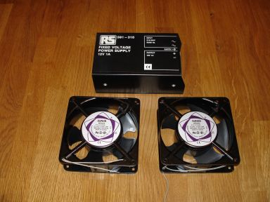
I was not confident about pure convection and so went for forced air
cooling using mains fans, again from Ebay.
Power
Supply
The
amplifier
runs of 50V and with 600W out will need about 1000W in, ie 50V at 20A.
To
power
this an ELTEK
brand new power supply off Ebay
but sold by Anchor
Surplus
in Nottingham is ideal. It is nicely protected and can be
started
up by a 5V control line. This allows it to be powered down on
receive to avoid nasty noises from the switching, although in practice
it seems to reasonably quiet anyway:
Auxiliary Power
I decided to use 12V for control systems to provide compatibility with
other systems I had. I got a 12V PSU, again off Ebay, shown
here
with
the cooling fans.:
If
you
are really interested (or is it sad?) then here is the
spreadsheet with all parts as
ordered
(except Ebay).
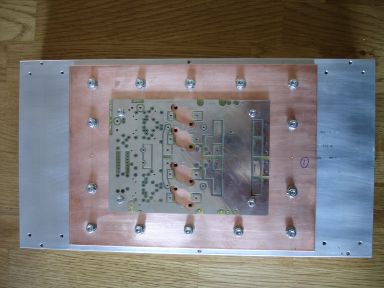
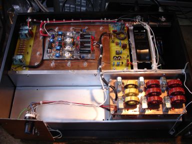
Main
Board Assembly
Before the board can be assembled, there is a great deal of mechanical
work to be done to mount the heat spreader onto the heatsink and then
mount the unpopulated PCB onto the spreader. Only when all of this is
done is it appropriate to put the components onto the amplifier board.
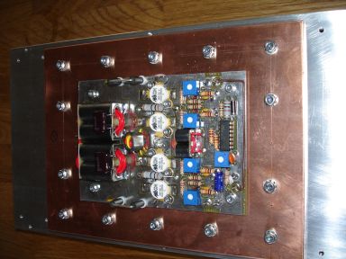
After much planning, drilling and tapping here is the PCB on the
spreader, with the spreader, on the heatsink. I found it
critical
to have a pillar drill to do this. I went and bought a
£55
one, new, from Machine Mart.
Here's the trial of the board on the spreader and heatsink:
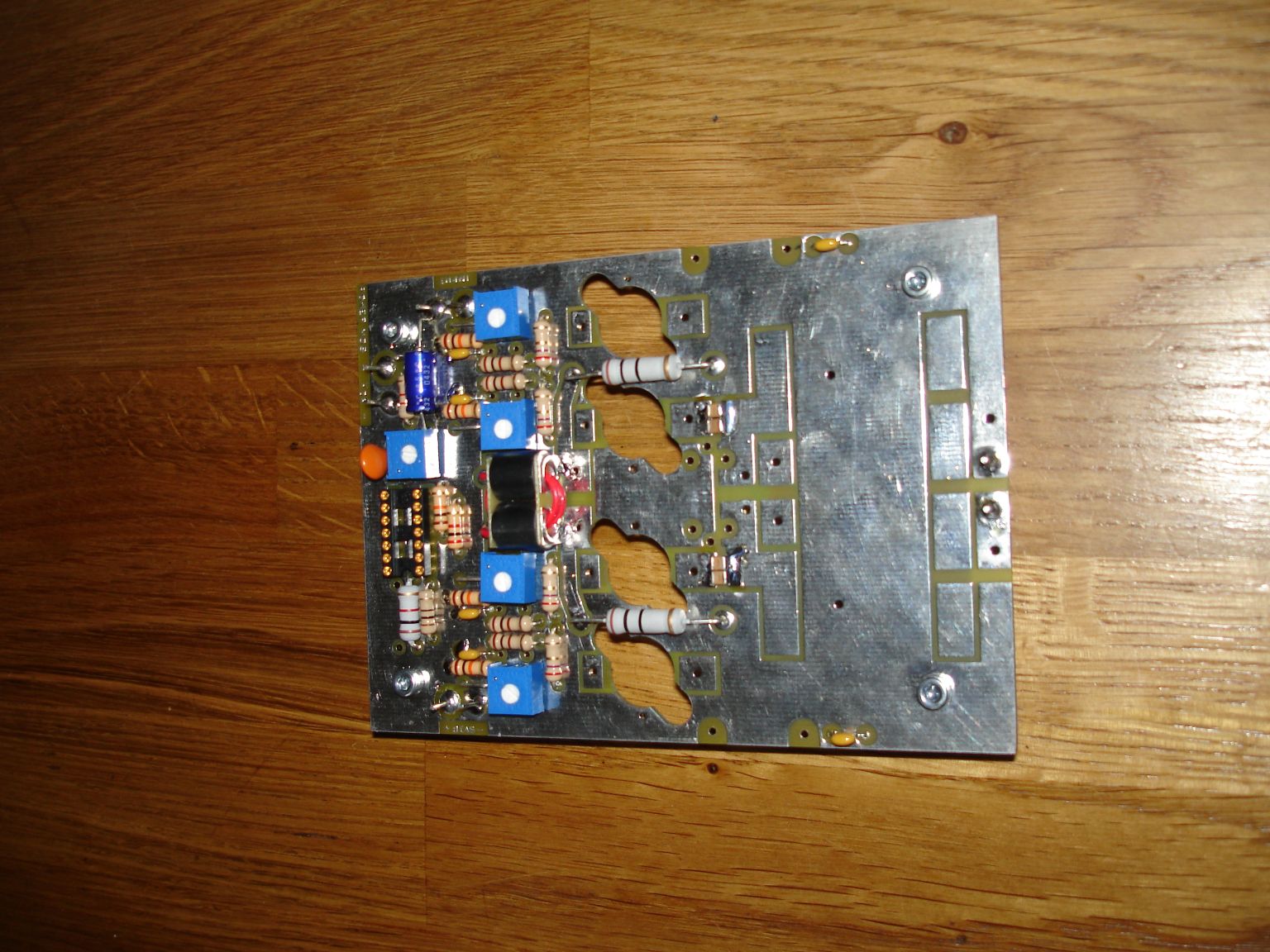
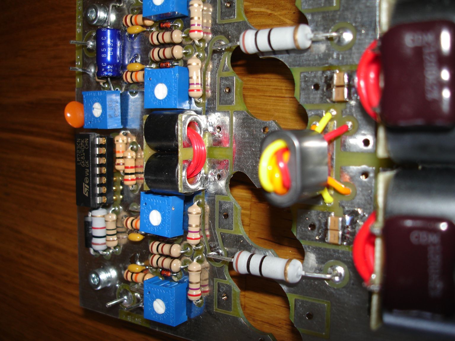
Population of Board
This
a fairly long winded process with components on the top and the bottom
of the board. On the bottom of the board are some chip caps.
The board needs to be just clear of the spreader to ensure
these
don't short:
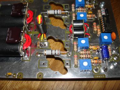
I next fitted the solder pins, and in retrospect the two big resistors
that are part of the feedback loop (below) should have been on pins, it
would make life much easier later on:
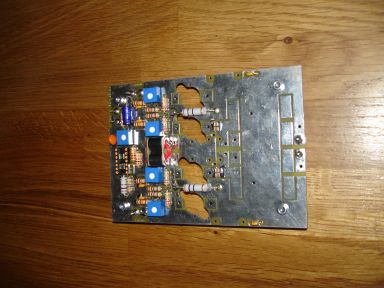
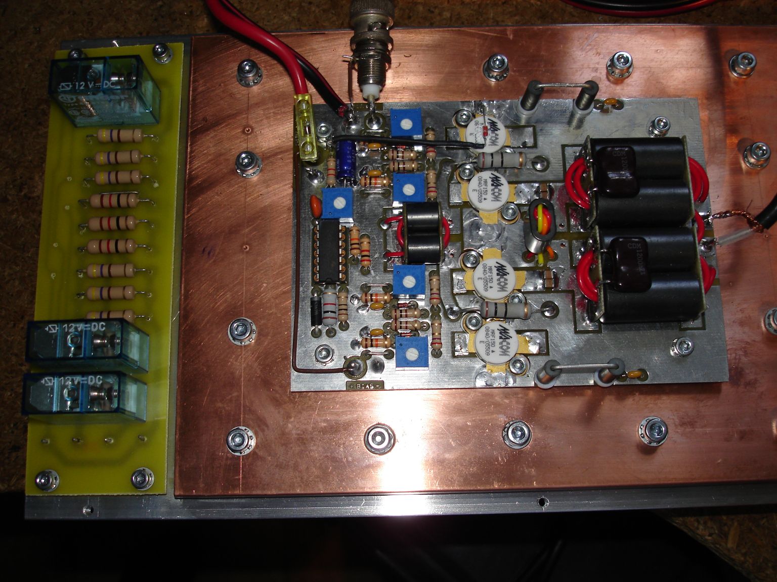
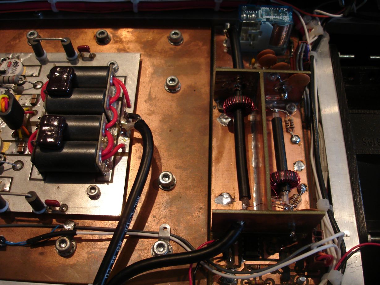
Putting the rest of components on gives:
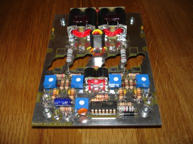
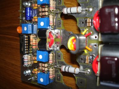
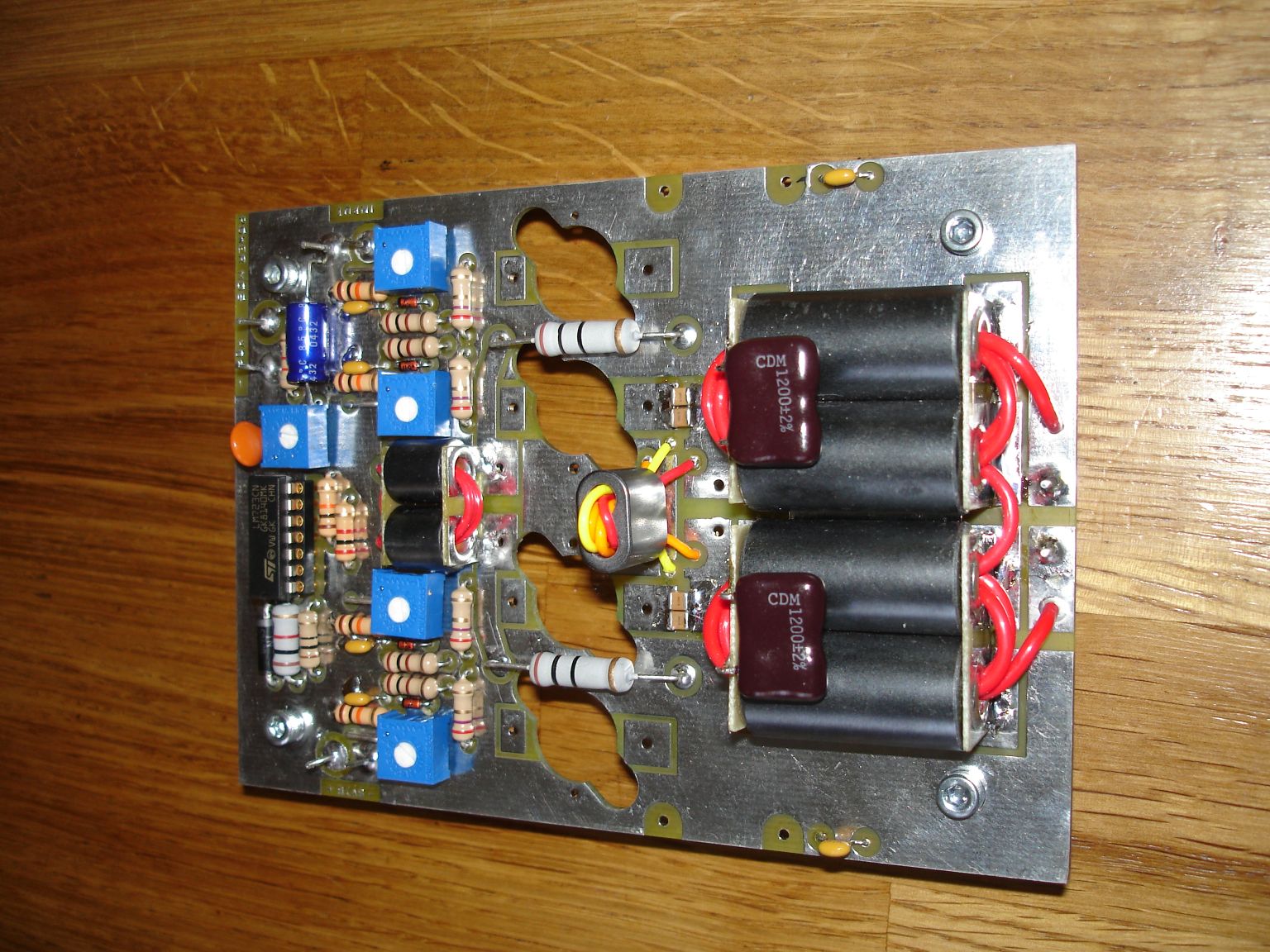
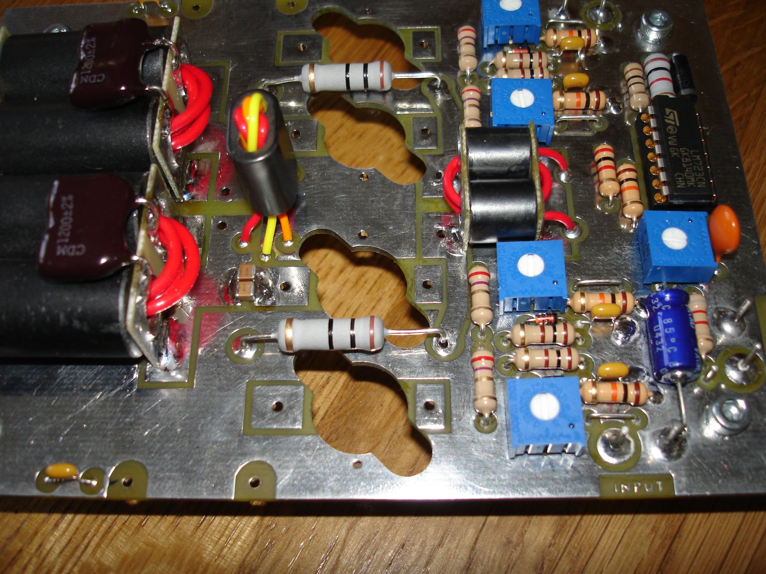
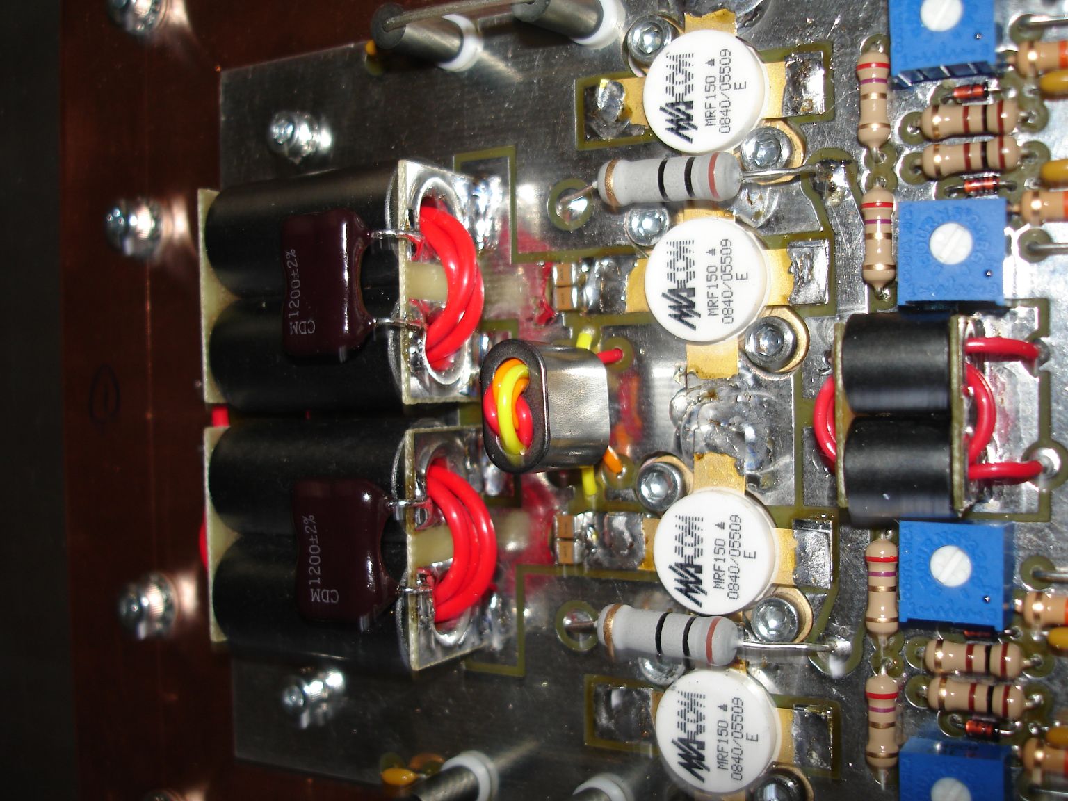
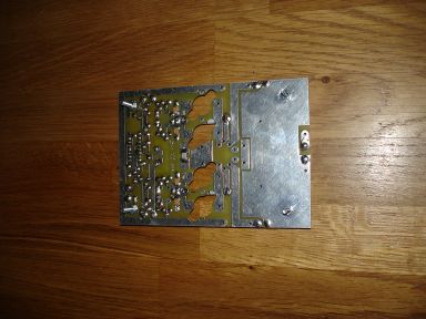
Power
Devices
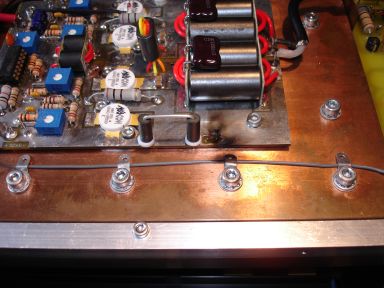
After various trial fittings, marking out, drilling and tapping of the
spreader and finally checking for shorts, the board was fitted to the
heat spreader and the devices soldered in:

Notice the 1W resistors have got a bit bent to allow access to the
device screws. Next time they will go on solder posts.
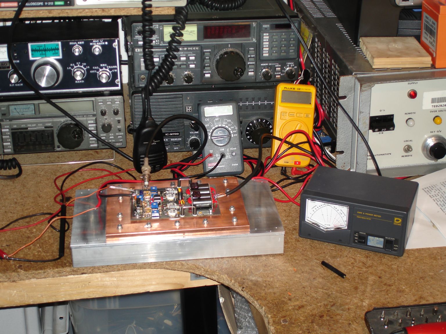
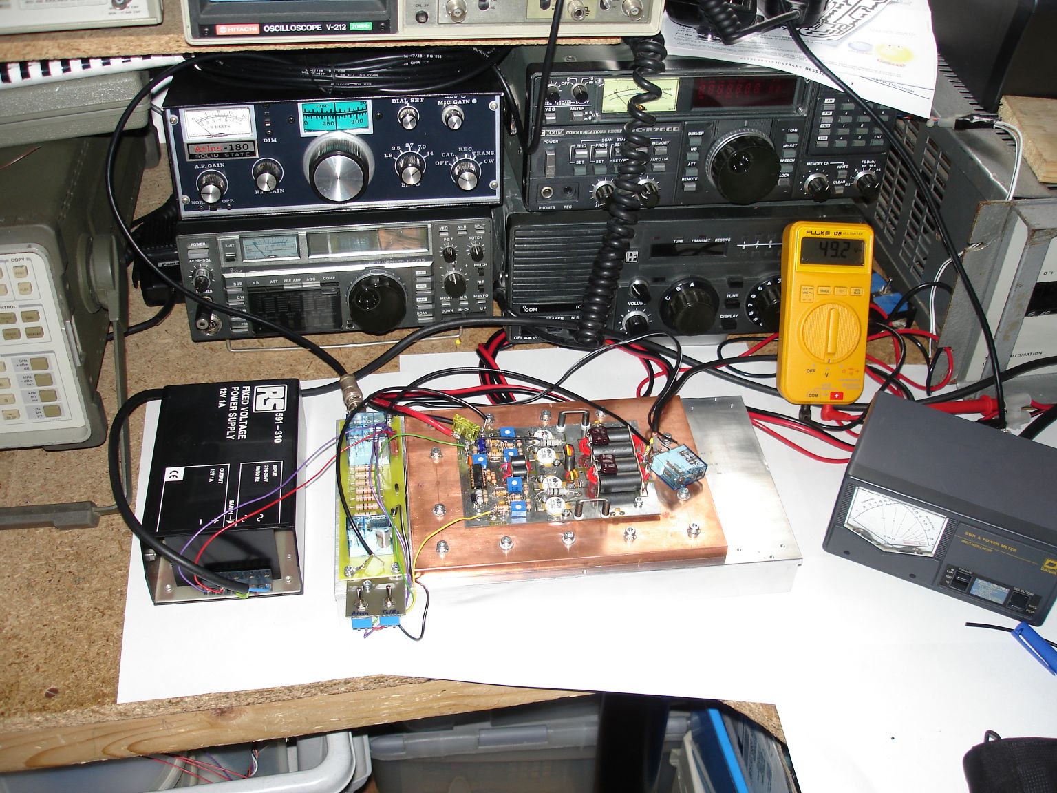
Initial
Testing and Bias Setting
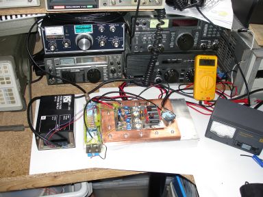
At this point I decided to be brave and put the supply on and,
hopefully, set the bias currents. I bodged up a 3A fuse (just
because I had one) and monitored both the voltage and the current.
I am fortunate to have a 0 - 50V, 40A variable PSU
which
makes life easier. Here is the bodge up of the first test:
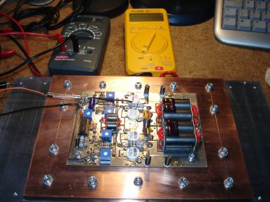
It proved to be pretty easy to set the bias current to 1A total, ie
250mA per device. As I was taking it up from the initial
supply
voltage of 40V to 50V as a check there was a bang, a blue flash and a
blown fuse - not good. It turned out to be a small offcut
strand
of wire across one of the devices. There is a lesson here
about
cleaning the board before testing!
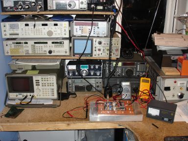
Gain
Test
The next check was to see if it amplified. I used a signal
generator which has a maximum output of 19dBm (ie about 100mW) at 14MHz
to see what would happen. Thsi produced about 5 or 6W into a
50
Ohm dummy load which seemed ok to me. The next check was to
use
an FT817 (out of picture) to provide some RF as this can have it's
output reduced down to about 100mW.

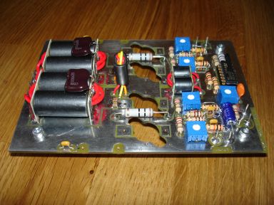
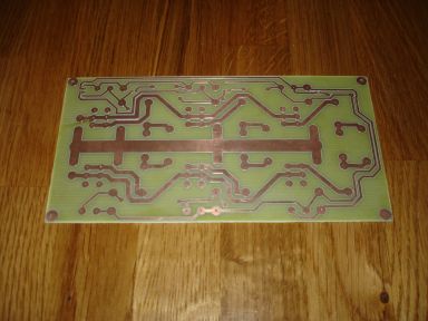
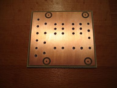
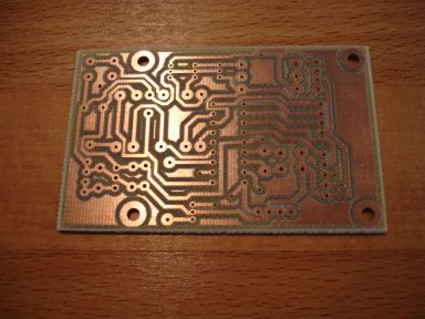
Attenuator
Board
Once I had established the amplifier board itself seemed to be working,
I designed the attenuator. The actual design of the component
values was done using WinAtt
from GM4PMK on G3SEK's webpages. I used TinyCAD
for the schematic capture, FreePCB
for routing the board and ViewMate
to
print to pcb out.
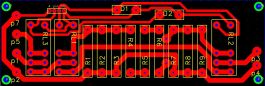
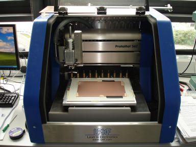
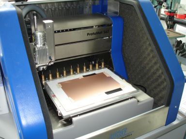
I
got
the board made at
work using a prototyping system
that uses a routing technique to
remove copper from those areas where it is not wanted:
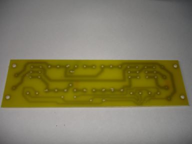
Another idea I investigated but did
not
really got to work properly is the
"iron
on" technique. The
finished, routed boards come out ok, but
are obviously not plated, but that I can live with:

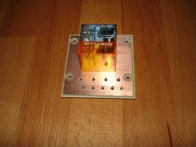
Here
it is populated, fitted but not
yet wired in:

I
then bodged on an output
transmit/receive relay and the 12V power supply to give a complete
working system:
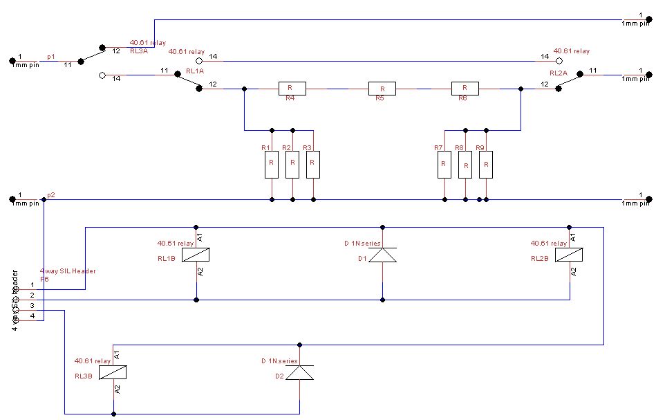
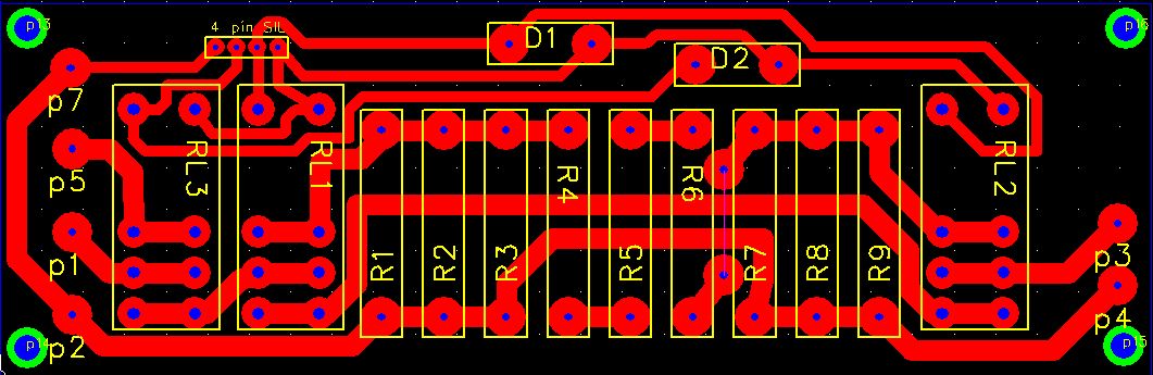
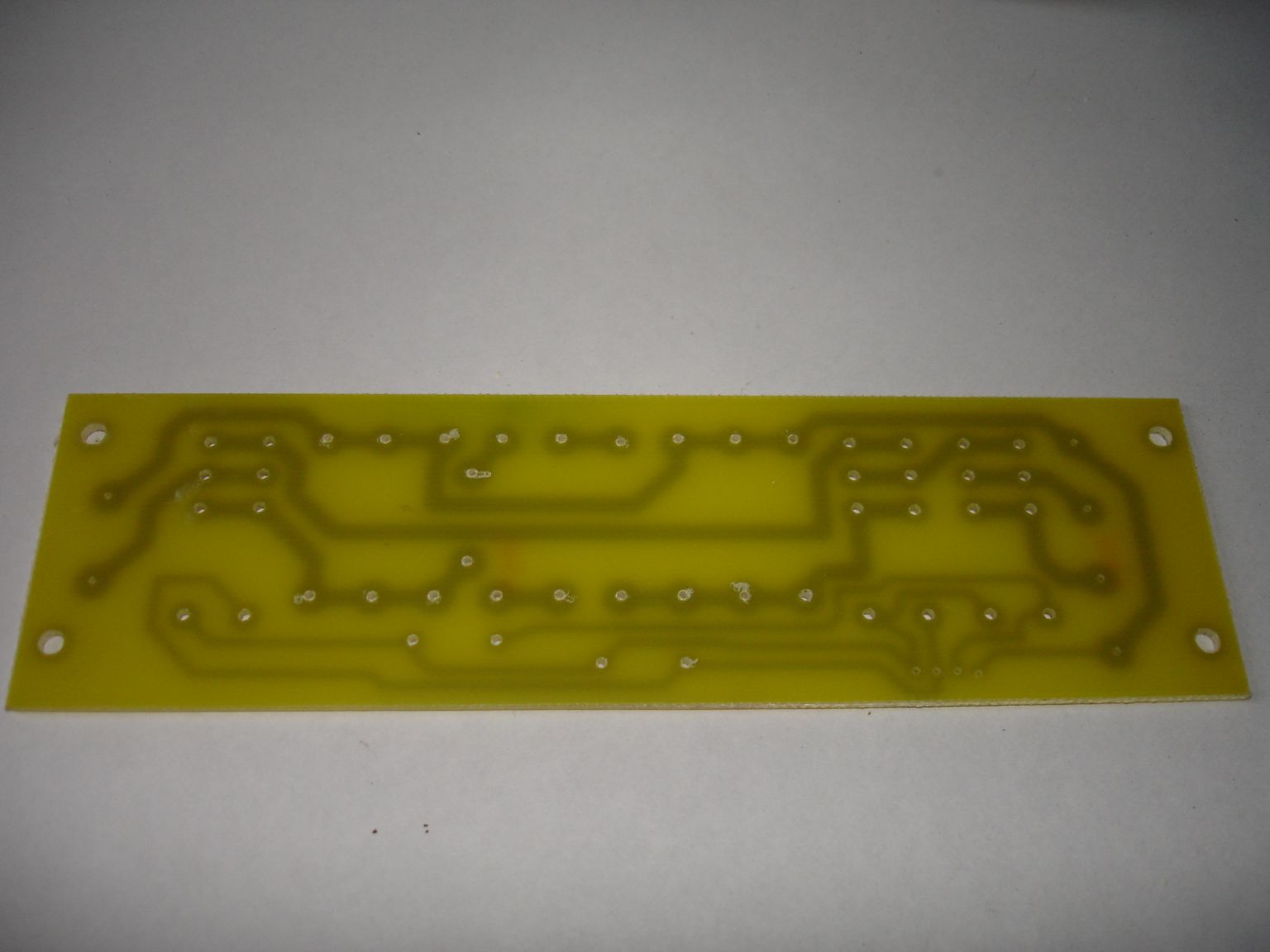
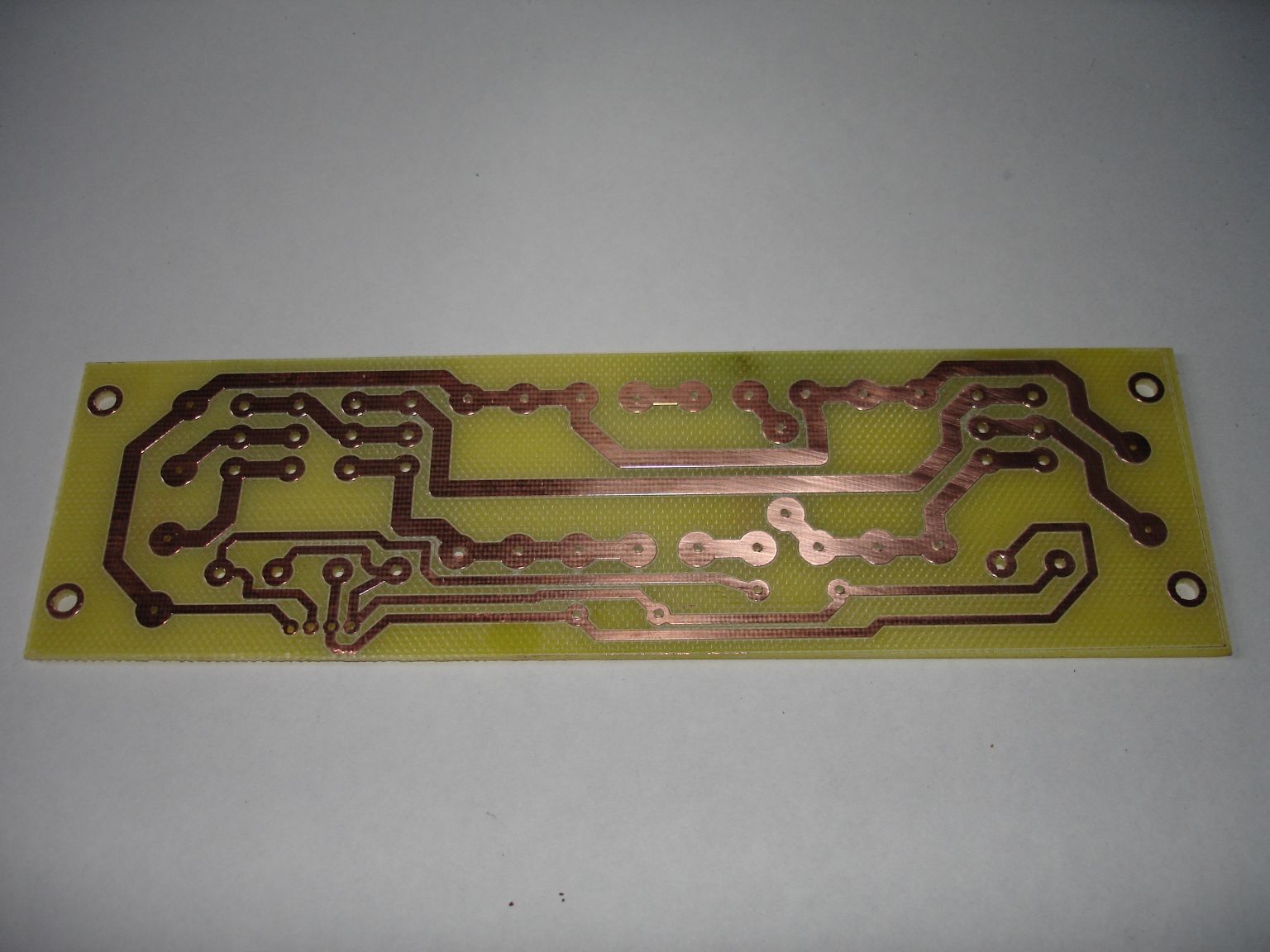
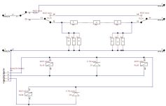
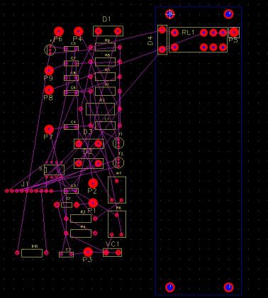
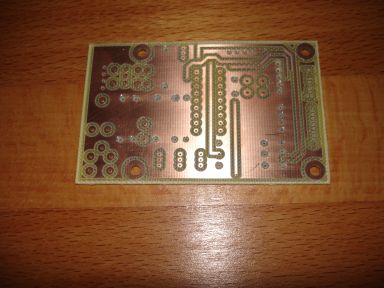
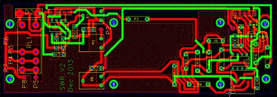
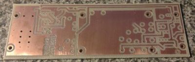
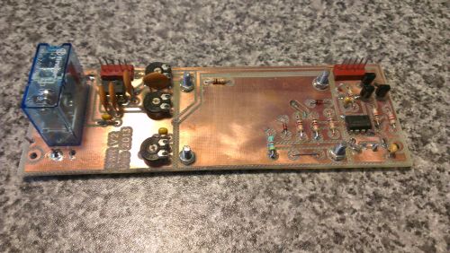
Output
Switching
and SWR Board
To
protect the devices it is clearly
necessary to shutdown the amplifiier in the event of high SWR, for
example a flashover in an ATU. Also a relay for
transmit/receive
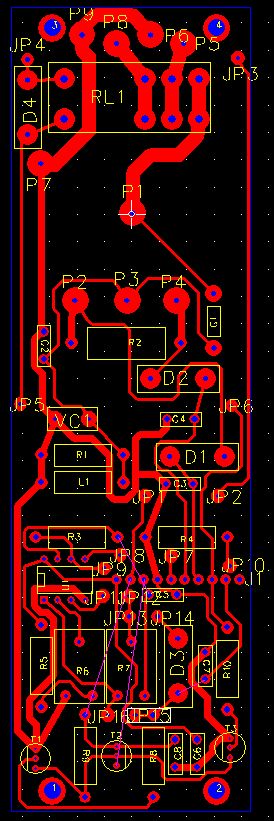
swithching ant the output is needed. I then designed a board
to
do this, it removes the 50V bias supply if it detects excessive SWR at
the output:. The PCB
layout starts as a schematic capture and is then imported into EasyPCB
to give "ratlines":

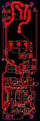
The
final result looks like:
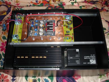
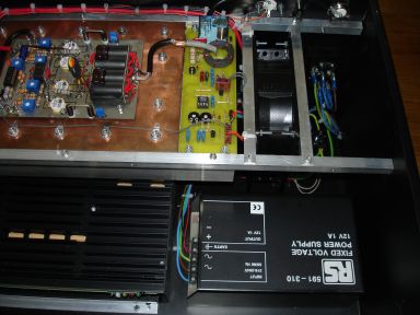
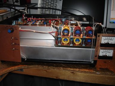
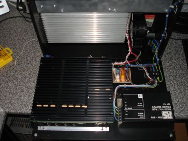
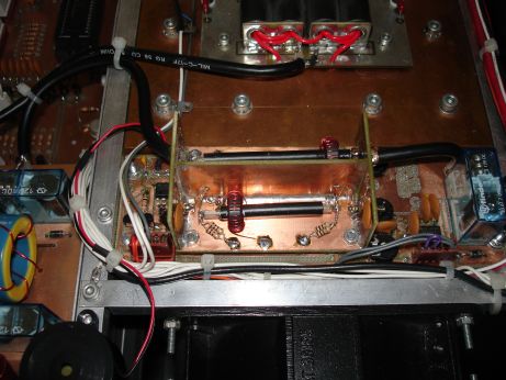
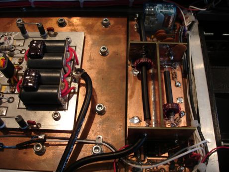
Mounting
in the
Case
Much
of the time was spent puzzling
out how to mount all the bits in the 19" rack mount case.
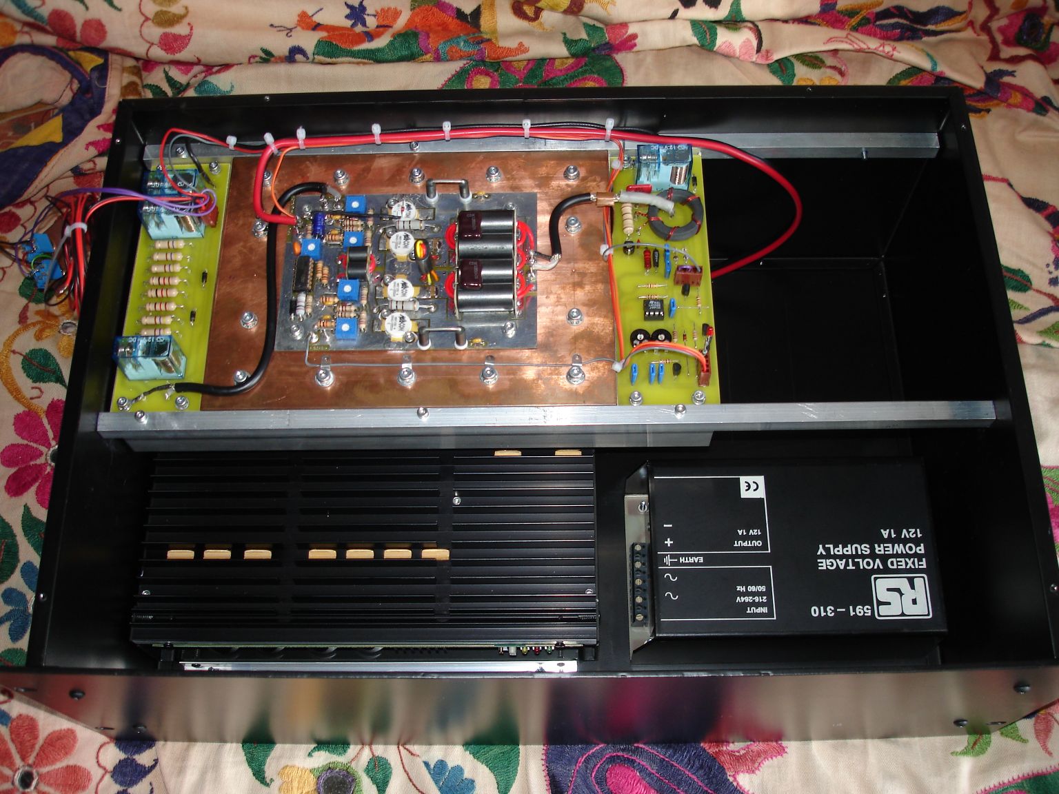
Here is
the stage with the amplifier, input and output boards and power
supplies mounted. The cooling fan, output filters and front
and
rear panels have not yet been dealt with.
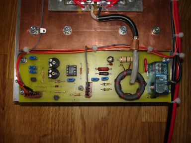
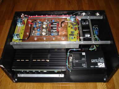
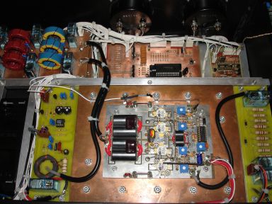
Here
are the major components
installed and wired up. The amplifier is now usable but is
minus
the output filters. Some low level instability in the
amplifier
disappeared with the input and output SO239 and fitted and the power
supplies properly wired in
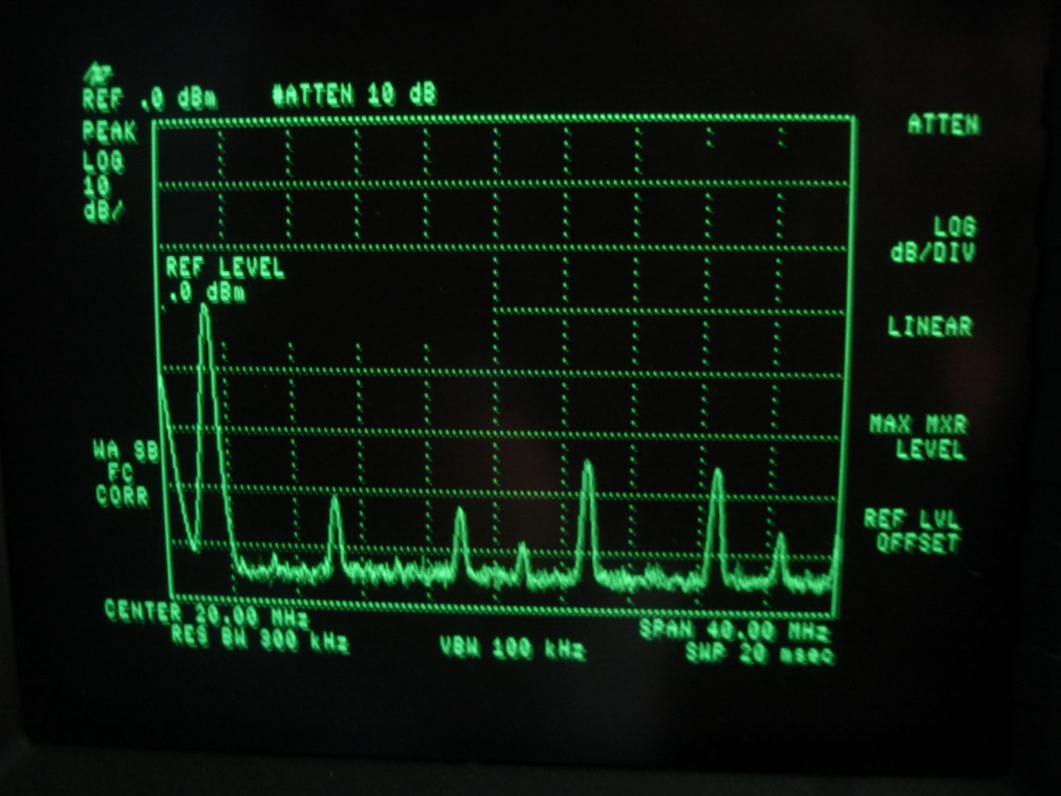
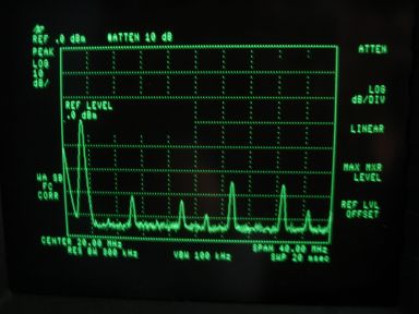
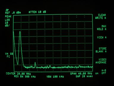
At this stage the lack of filters means the output was not
too clean, this was on 80m, some harmonics are only some 25dB down on
the fundamental:
The other lesson is not to push things to hard. The bypass
caps
on the drains supply don't like too much RF current. While
trying
to see how much power I could get out of it I discovered they go bang
and burst into flames. Here is the aftermath of this
happening,
the remaining leads in the plated through board were very difficult to
remove.
It seems as if too many harmonics are the problem which leads nicely
into the design of the output filters.
Filters
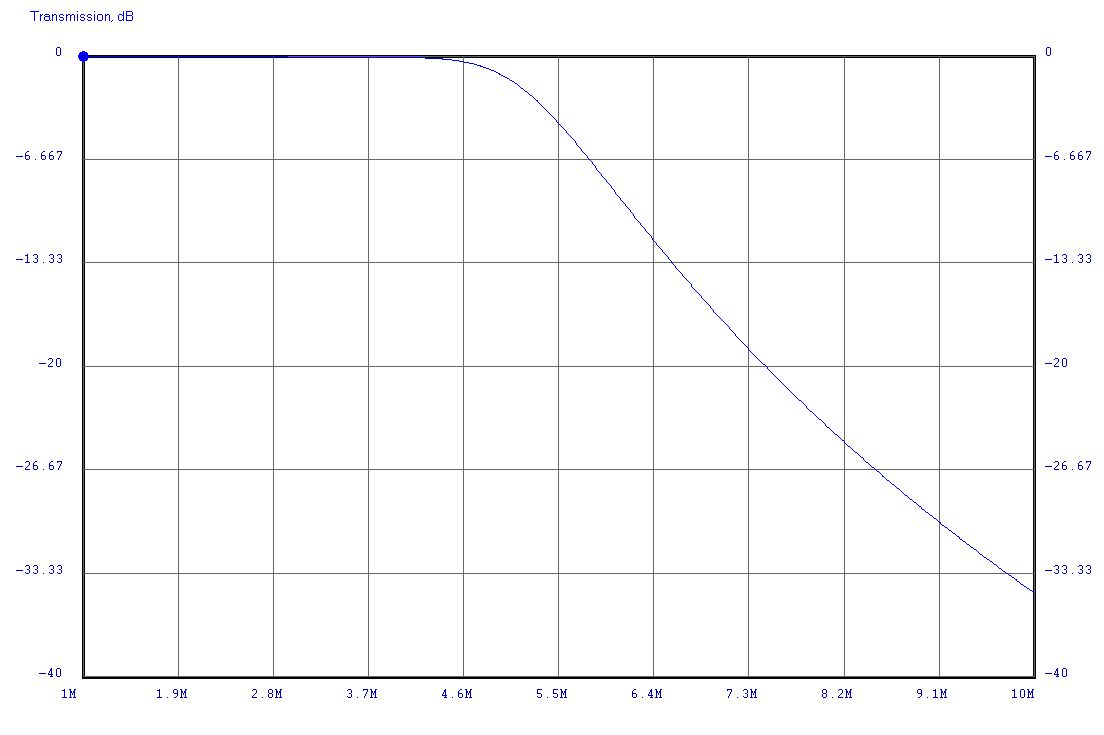
It seems to be fairly well established that a 5th order Chebyshev
design is appropriate for removal of harmonics from power amplifiers.
The design of the filters was based on the ARRL
Standard Value Capacitor
(SVC) tables. Once
the values had been calculated they were
modelled using ELSIE.
Using information I already had (not
sure where it came from) it became clear that a T-130-2 ferrite would
handle the power and provide the necessary inductance. An
example
of the design process is given in this
document.
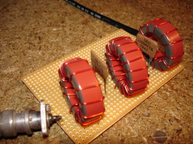
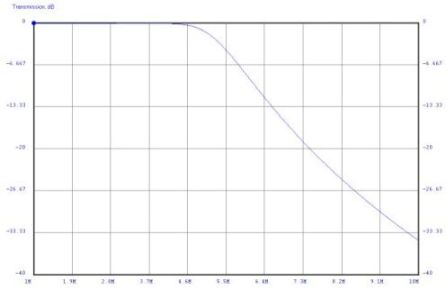
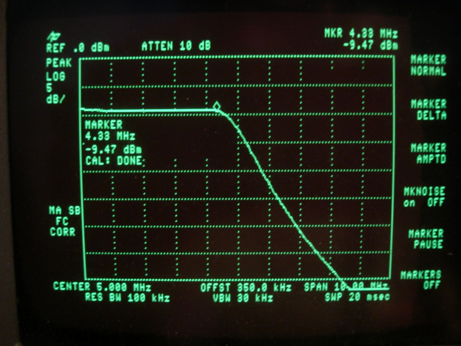
I
put together a prototype of the
3.5MHz filter as well as simulating
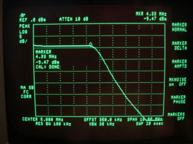
it: I then used a Panasonic VP-8191A signal generator plus a
HP8590A
spectrum analyser set to peak hold to find the filter's response:
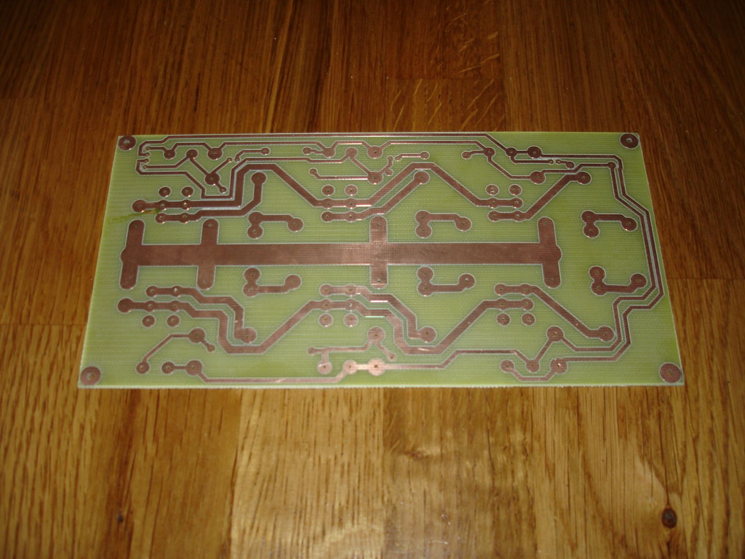
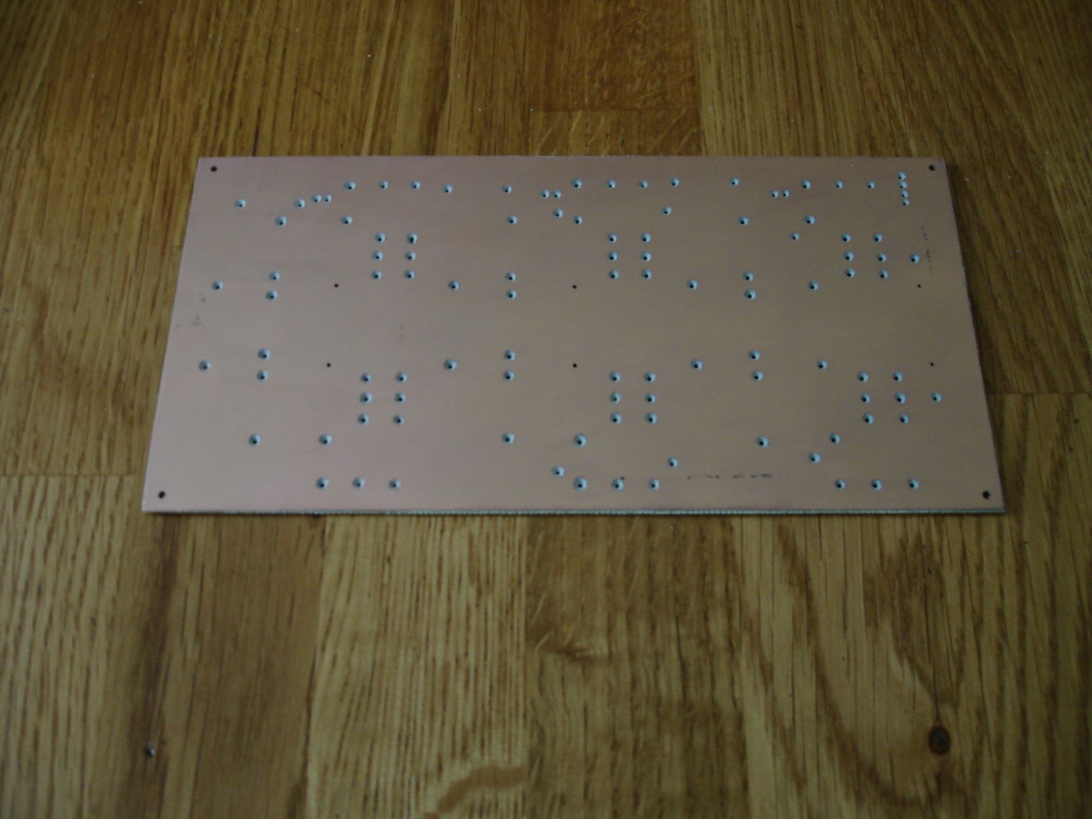
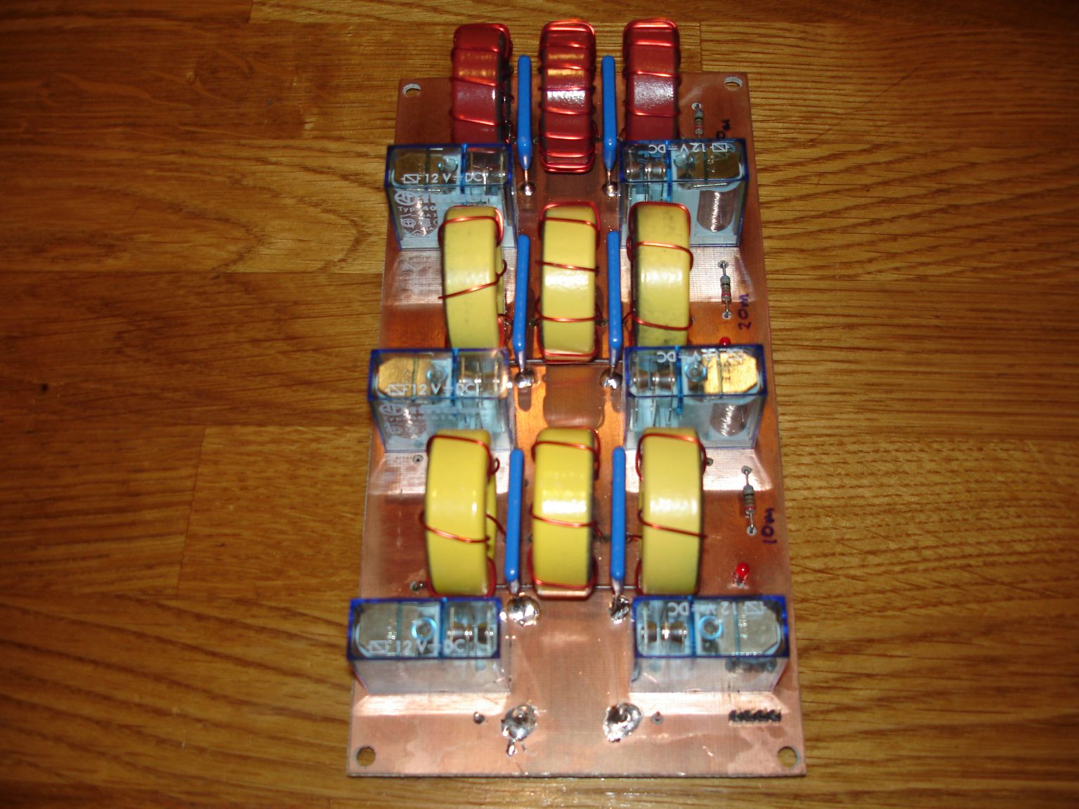
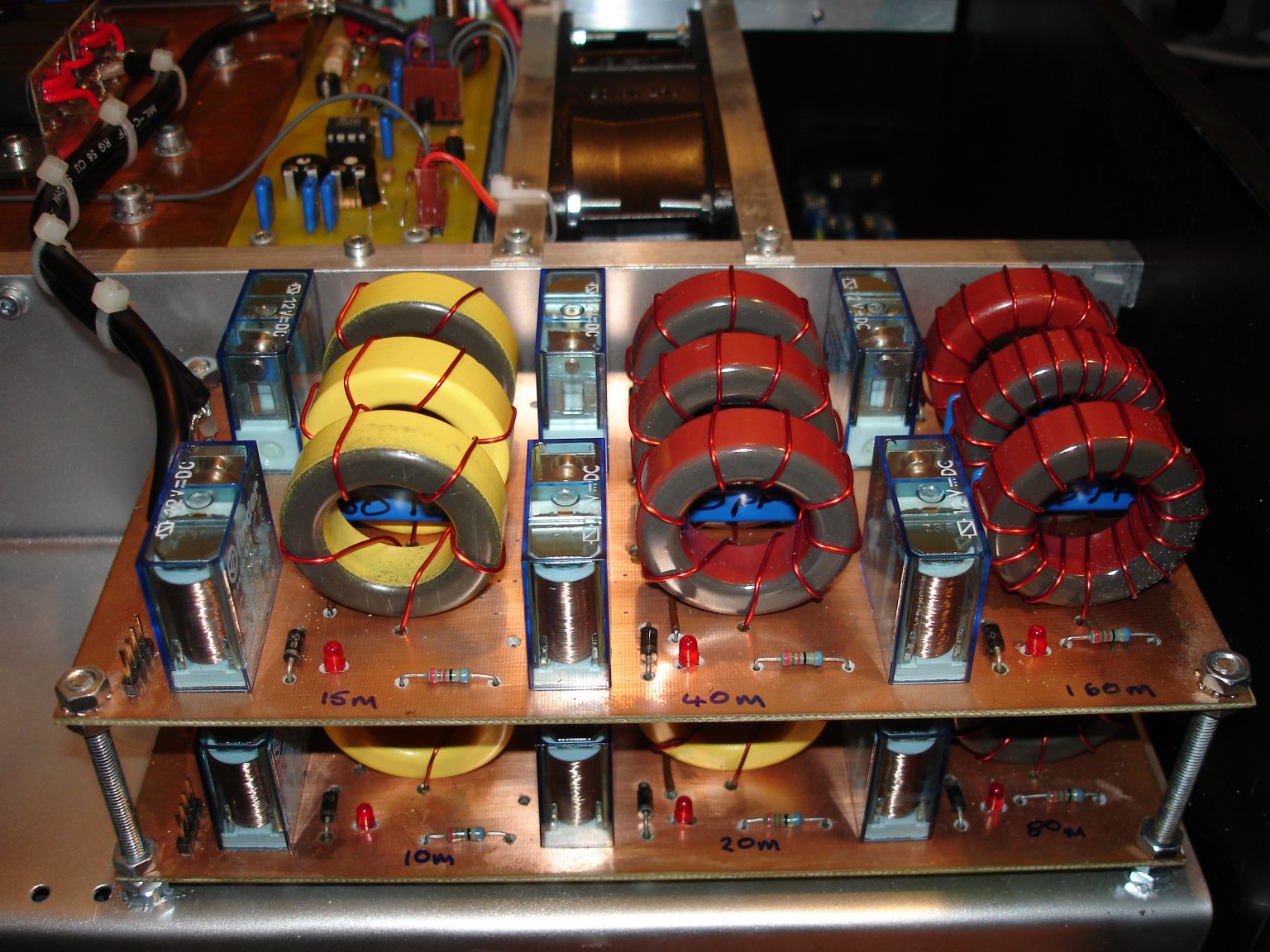
I
decided to put 3 filters on a PCB
and then use 2 boards to cover all bands. This was in an
attempt
to keep the track lengths acceptable. It seemed a bad idea to
have lots of RF going down long tracks. The higher the
frequency,
the shorter the track ought to be. I used an earth plane
approach in attempt
to cope with the potentially high RF currents. The unpopulated boards
look like:

And once populated and the topband filter tested:

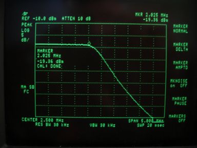
The second board was built and tested. I then stacked them
using
some M3 studding and wired it all up:
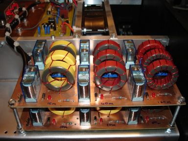
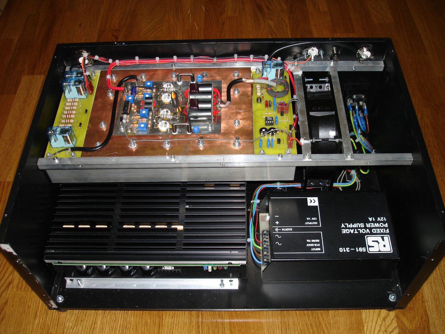
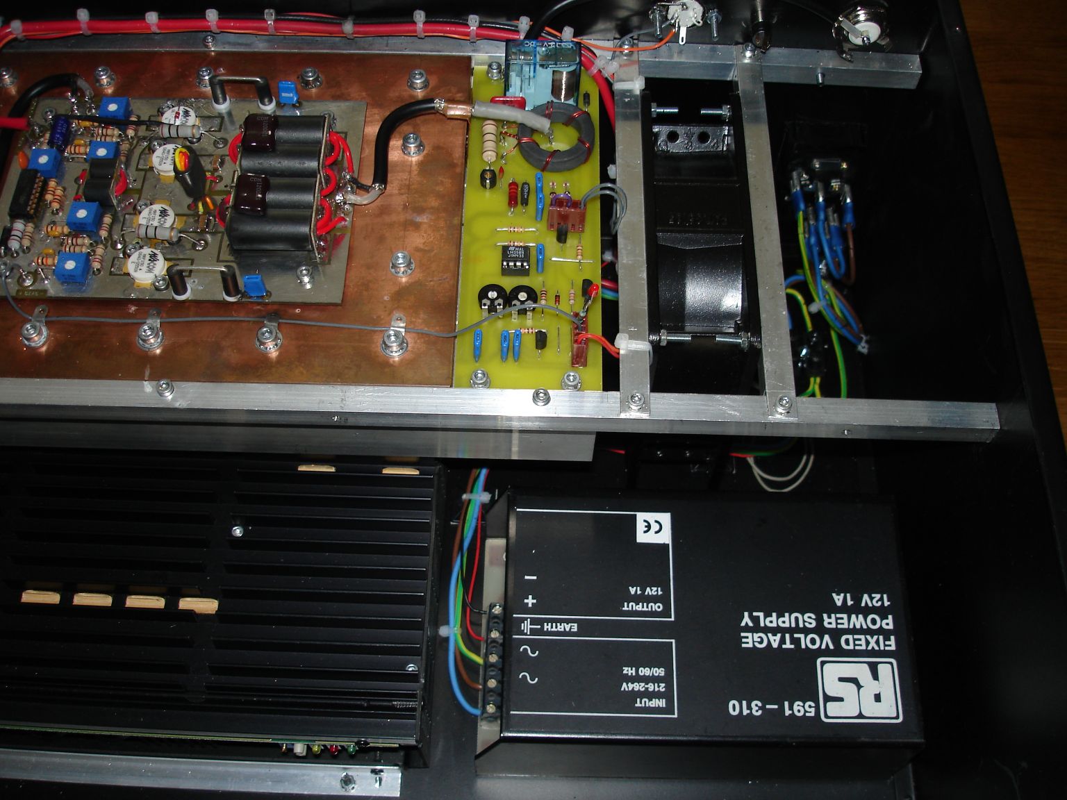
These photos also show the tray made out of bend and painted steel that
carries the boards and acts as a duct for the cooling air.
The
left hand side where the space is is where the control board will
eventually go.
Using the amplifier on
160m
and 80m at about 350 - 400W it
developed a fault where it would become erratic on transmit.
The
power output would disappear and then reappear. This did not
appear to be related to band, drive level, output power level etc.
At this stage I bodged on some meters to watch the supply
voltage
and current (see below). Of course it did not do it again
although I did
get it to smoke while giving it a long wwwaaaahhhhh. I
suspected
that the PSU was going into some sort of shutdown, but not due to over
current as the drive level did not affect the problem. I
suspected
RF getting into the control circuitry of the PSU.
Monitoring the voltage
and
current
soon showed the problem was not the PSU. Putting an old SWR
bridge
onto the input showed a very poor match and that the drive from the
IC735 was disappearing when the problem occurred. My
conclusion
is
that rig was shutting down as it got warm due to a poor mismatch (or is
that a double negative?). The solution is to run the IC735
via
the 6dB
input attenuator so that it always sees a good match. The
problem
has
not happened again since keeping the attenuator in all the time.
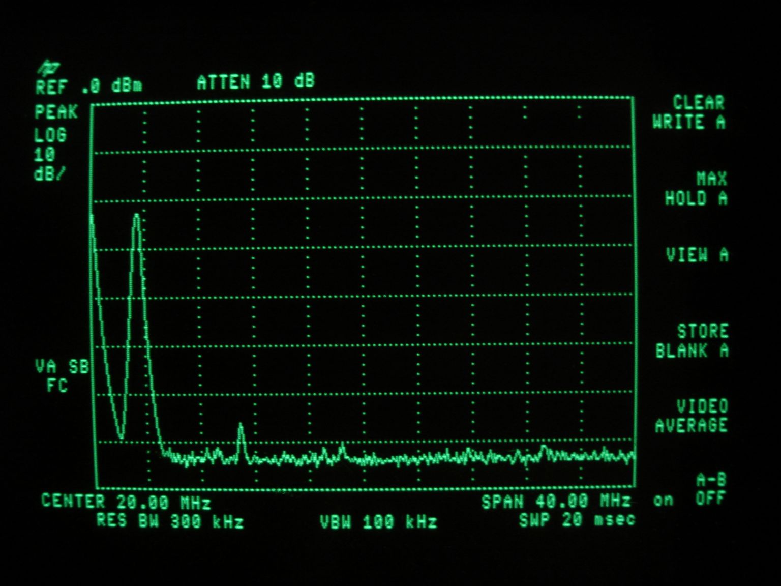
However the filters do seem to be working, the second harmonic is now
some 45dB down on the fundamental on 80m. Compare this to the
earlier plot of no filter which had the fundamental only 25dB down.
The filter should, at about 7.5MHz provide about 20dB of
attenuation so, surprisingly, it seems to do wha the theory says it
should! The third harmonic now seems to have gone - good.
Front
Panel
At this point I started to look at the front panel design and the
associated control circuits to select the filters, attenuator etc.
I decided to go for "push to select" approach rather than
rotary
controls. Rotary controls and toggle switches could have been
connected directly to the relays etc but but aesthetically this would
have look amateur and I want to have a reasonably professional end
result. This will imply some form of logic to interface the
buttons to the relays etc.
The front panel is made from mainly off the shelf parts from
Farnell but the meters are from a rally.
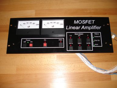
The front panel layout was done using free software from Front Panel Express.
I used
this as it is intended for front panel work and so the dimensions and
positions can be easily controlled. I am fortunate to have an
office that is directly opposite the Graphic
Design
student's printing workshop, so I went and talked nicely to the
technician and got the screen printing done...... The
printing is
water based so I lacquered the blank panel to protect it.
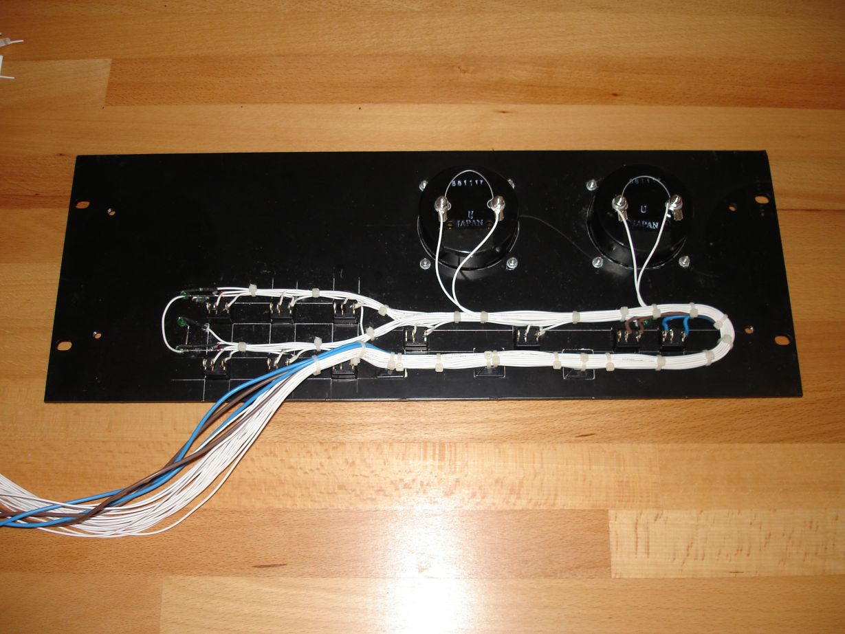
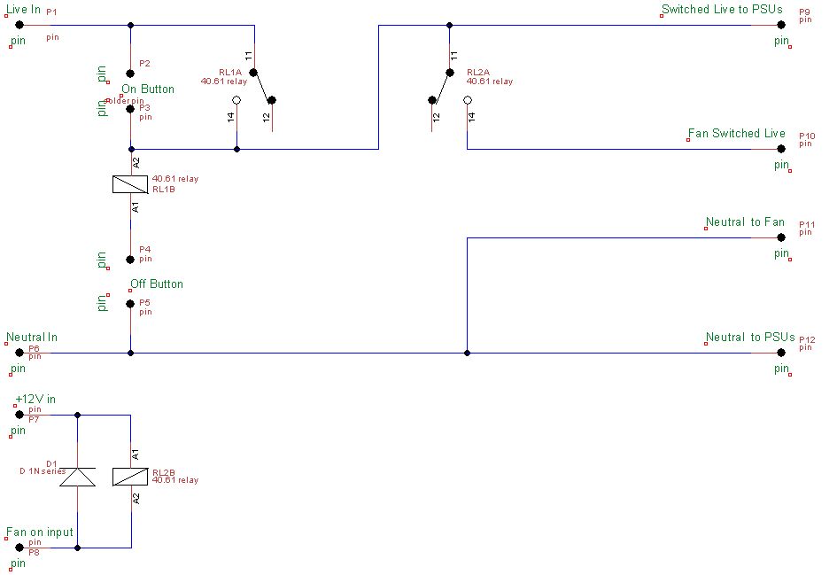
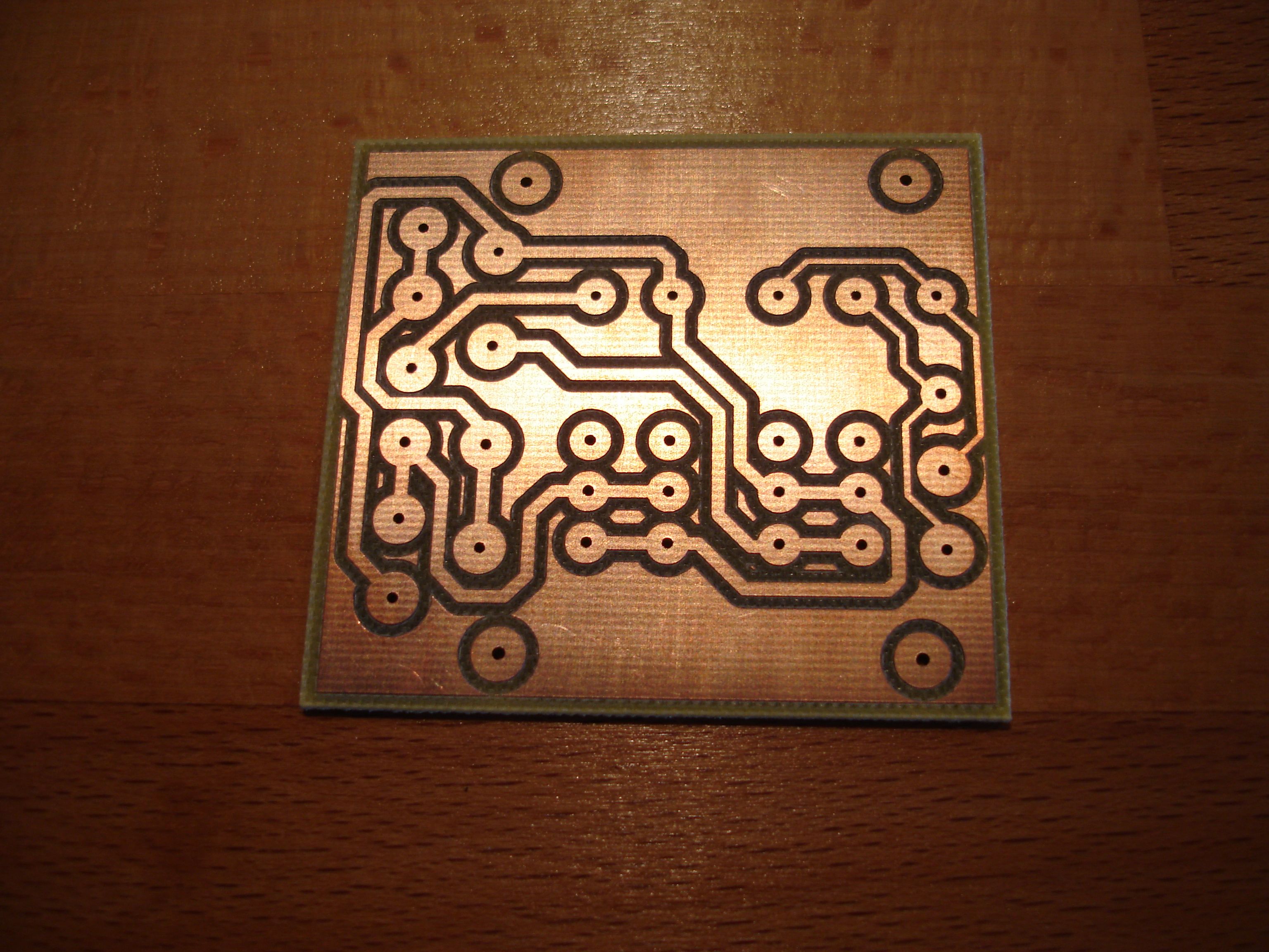
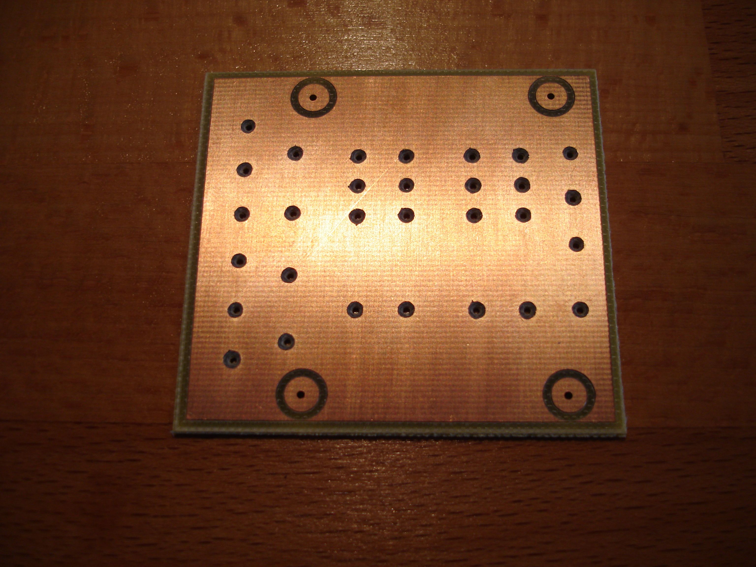
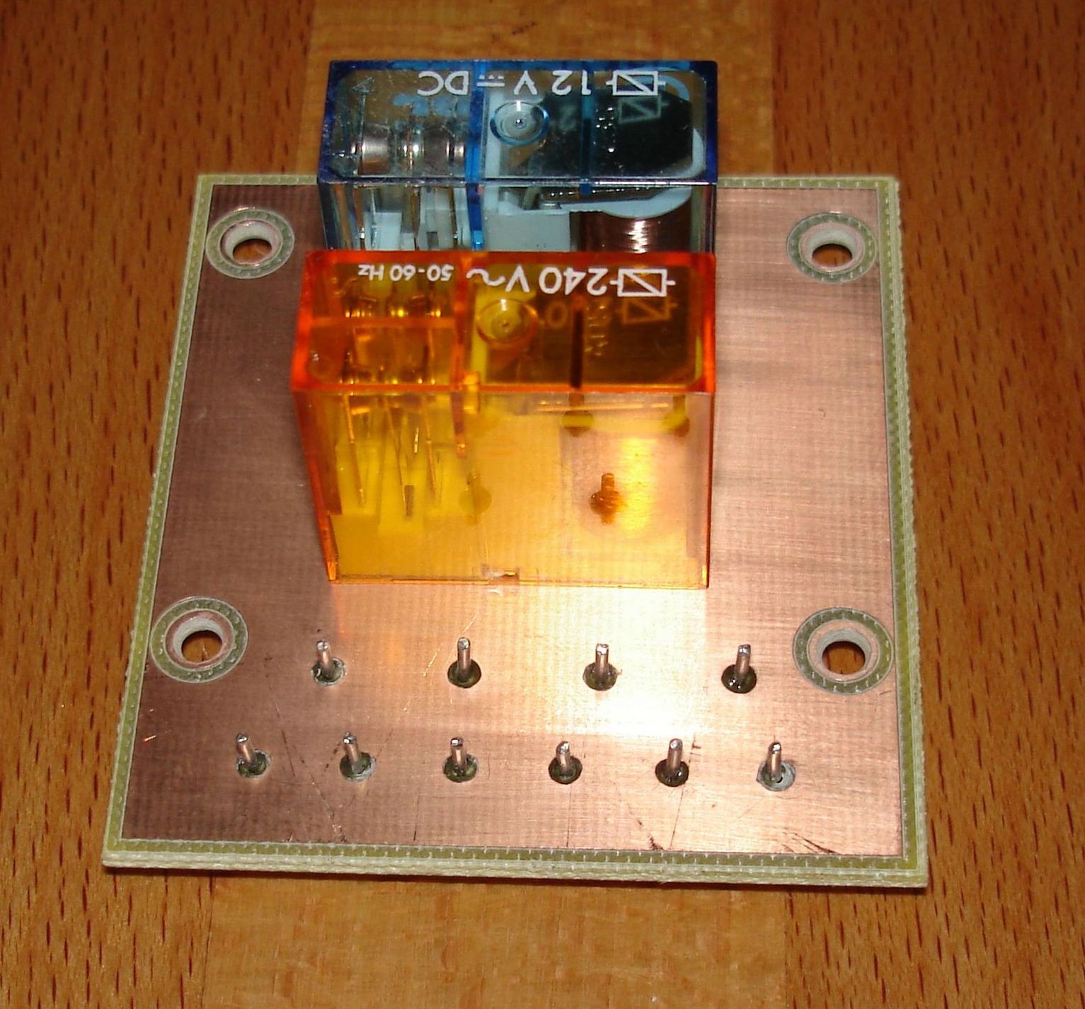
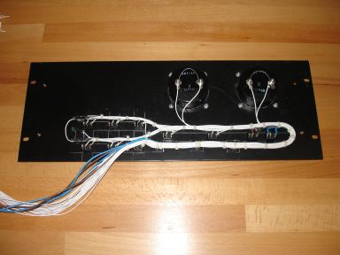
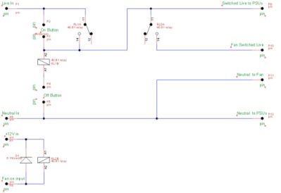
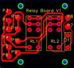
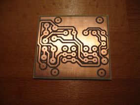
Mains Board
I
wanted a hard on/off with complete
isolation of the live from the psu when the amp was off. I do
not
like the psu to but in some sort of shut down mode. It is too
easy to end up with the supply on when you don't want it. The
on/off buttons feed a pcb with a mains relay that latches via
the
front panel buttons:
I've put this onto a pcb for neatness:
Here it is in place on the base plate next the 50V and 12V PSUs.
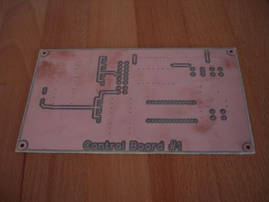
Control Logic
I thought I had a few options for the control logic each of which had
pros and cons:
- hard logic - significant
design
effort, hard to modify later but potentially simple and no EMC problems
- microprocessor -
significant
hardware and software design effort but flexible and I have programmed
in assembler before. Potential EMC problems from the clock
- Raspberry
Pi - this was a late
consideration. This met all my
connectivity, processing power and cost requirements BUT is
hard
to mount (no mounting holes), lots of cabling in strange positions to
cater for and, most importantly, it would need programming in a high
level language, probably C. I have no competence in any high
level language and accessing I/O ports is more complex - this was the
killer for me.
I
went for option 2 and chose a
PIC
as all the tools for generating the
code and loading the code onto the PIC is cheap and well documented.
After a lot of thinking I went for a two chip solution.
The
idea was to separate the control of the purely digital interface of the
front panel to the relays from the analogue functions (over
temperature mainly) and the comms function. I
intend to
include a CI-V interface to interface to my Icom radios so that the
amplifier is automatically on the correct band. It might add
Yaesu CAT as well if I can be bothered later on. For the
digital
interface I chose a 16F57
as this had the necessary number of digital I/O lines. To
date I
have been happy with this choice, with one exception. I
thought
it could
use ICSP (In Circuit Serial Programming), in fact it must
use this
method. This had the slightly annoying effect of
needing an
extra socket attached to my programmer.
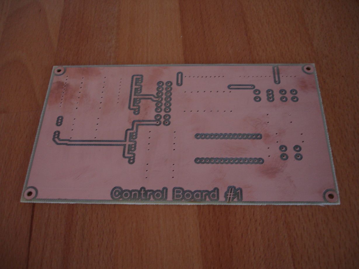
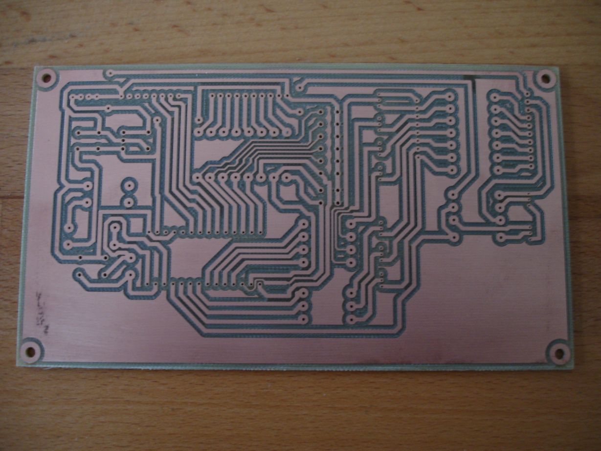
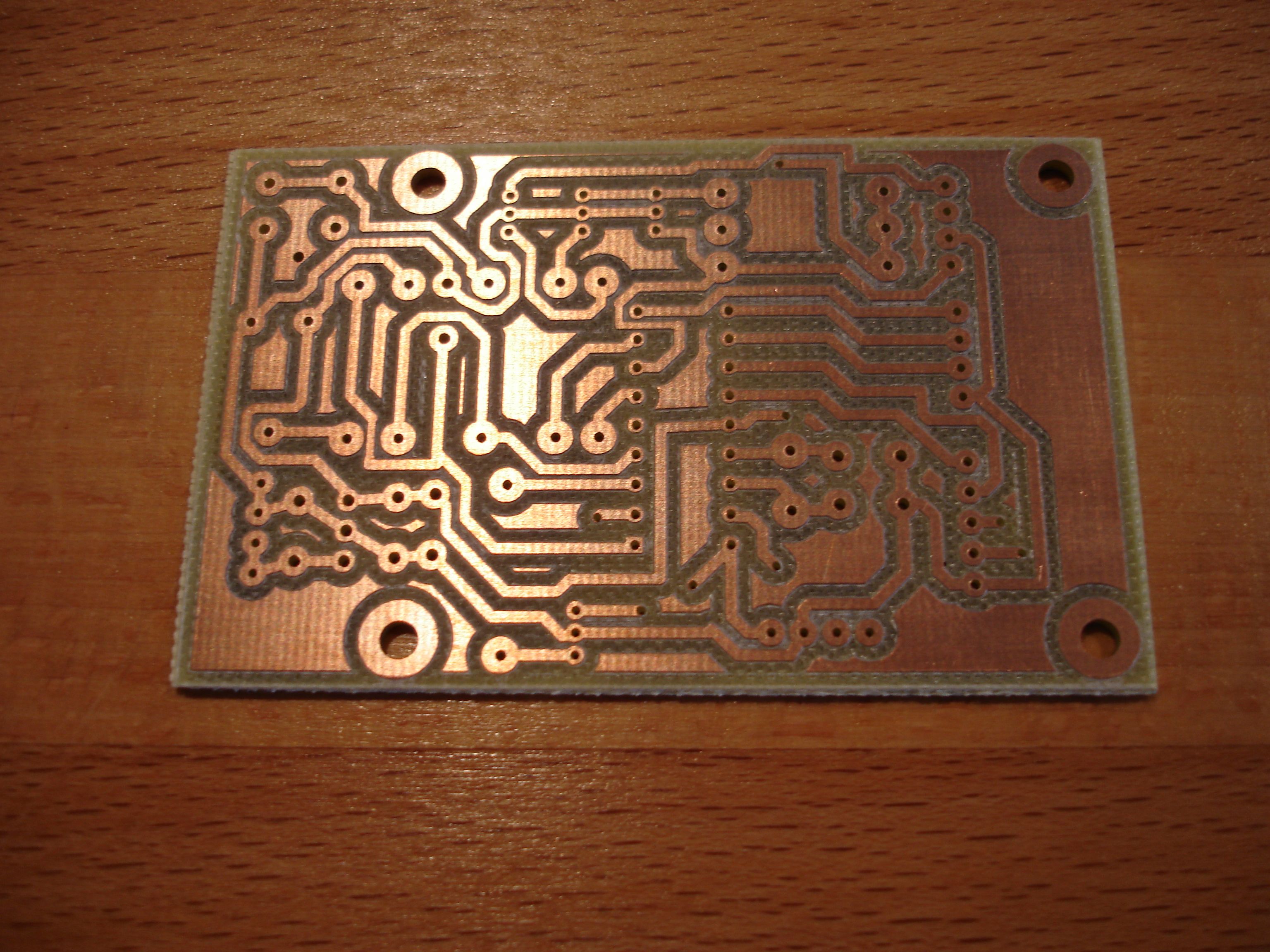
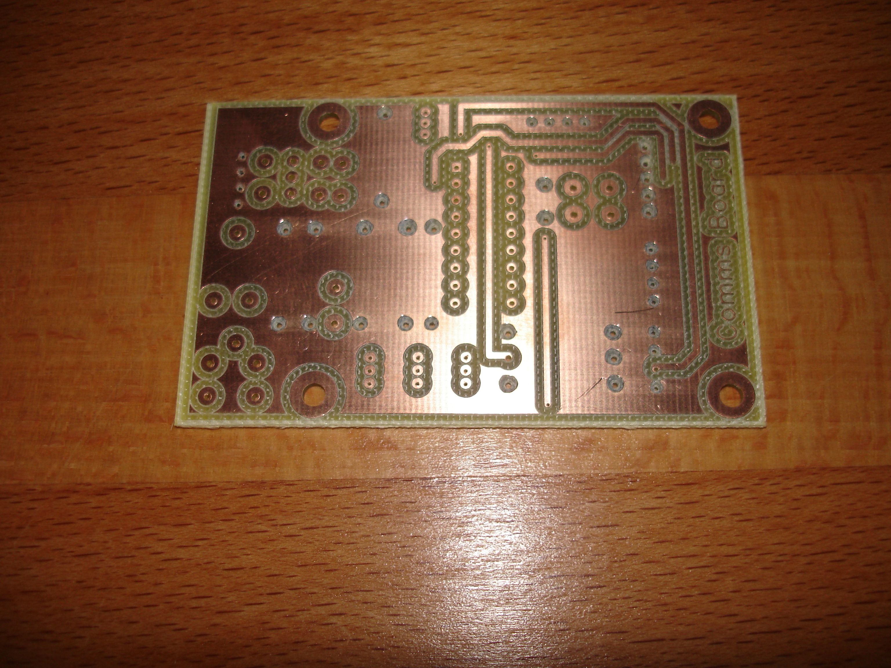
I designed a board using Tinycad and FreePCB as before.
FreePCB
has some problems in terms of producing the Excellon drilling file.
It seems to generate non compliant code. I checked
the code
using gerbv
and
hacked it (it's a text file) by hand until I cleared all the errors.
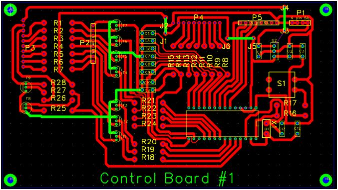
This is a double side board, but the top side only has a few links on
it. It was produced on the LPKF system as per the other
boards:
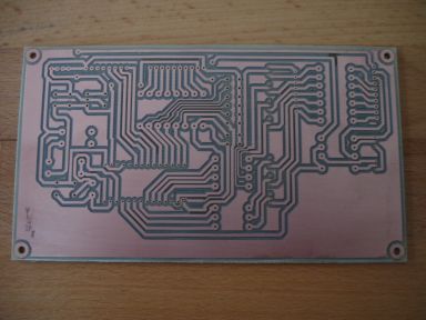
Having populated it and used it I would, in retrospect have done it
differently. I would have use SIL resistors to improve the
packing density, put ICSP on the board and put the digital controller
and analogue/comms PICs on the same board. The only problem
is
the sheer number of bus lines takes up a great deal of real estate and
I am loathe to use tracks that are too narrow as this is, effectively,
a prototype so hacks may be necessary - much easier on big tracks.
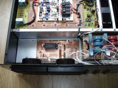
Here is board in the amplifier fully wired up:

In terms of writing the
code
for the PIC I used MPLAB IDE v8.86 available from Microchip
as a download. In
terms of how program, the manual
for the 16F57 is good, but you need more than this unless you are
really experienced. I used some ideas from here
and
most usefully from Gooligum Electronics who provide very good tutorials
which
should get most people going. To load the code onto the PIC I
used a Quasar Electronics 3128
PIC programmer but with a Vero
board extra to allow me to use ICSP
on the chip.
Version
one of the software
is now working, this provides control of the band, attenuator and
amplifier on button. The code is not sophisticated,
at this
stage I just wanted to get it working. This document
details the how the
PIC interfaces to the board. The PIC is now programmed such
that
the
board works correctly as the front panel interface for manual control.
It also now has the code to allow the second controller board
to
override the manual settings when it is automatic mode where the band
is set from the CI-V input from an Icom radio.
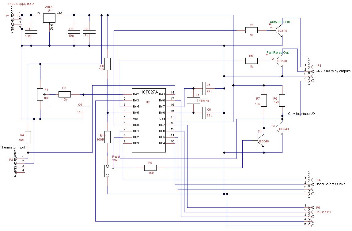
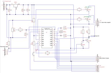
Communications Boards
This is the second processor board and it provides control of the
cooling fan based on the temperature and also will ensure the amplifier
automatically on the correct band. It will do this for Icom
radios initially. This is because I understand the Icom CI-V
bus,
have several Icom radios and finally I can't be arsed to do it for
Kenwood or Yaesu at this stage. The slow bit was writing the
code for it. I am
conscious that this will be time critical code so I will need to be a
bit more careful to avoid timing issues when programming the PIC.
The PIC I chose is the 16F627A as it provides the analogue
comparators needed for the temperature control as well as having the
UART needed for the CI-V interface.
Here's the design:
Currently I have got the
16F627A configured to use a comparator to turn
the fan on and off based on the temperature as measured by the
thermistor. This sounds simple but the different internal
architecture and the sheer number of configuration options meant it
took me a day to get this code working correctly. The nice
thing
is that now that this code is done I have a completely working
amplifier, albeit in manual mode only.
The auto band switching code is now written and working! It
proved to be easier than I expected the only the thing that caused any
problems was failing to set the global interrupt enable - that tends to
stuff things. If you really are interested then here is the
working code for control
board #1 and control board #2.
If you want to use my code that is fine but I would appreciate
acknowledgment of this if you in any way publish your code.
To
write the code a good understanding of Icom's CI-V code is needed, I
used a very old paper document that describes it for the IC735 but you
can find suitable information from Icom
or with a users perspective here.
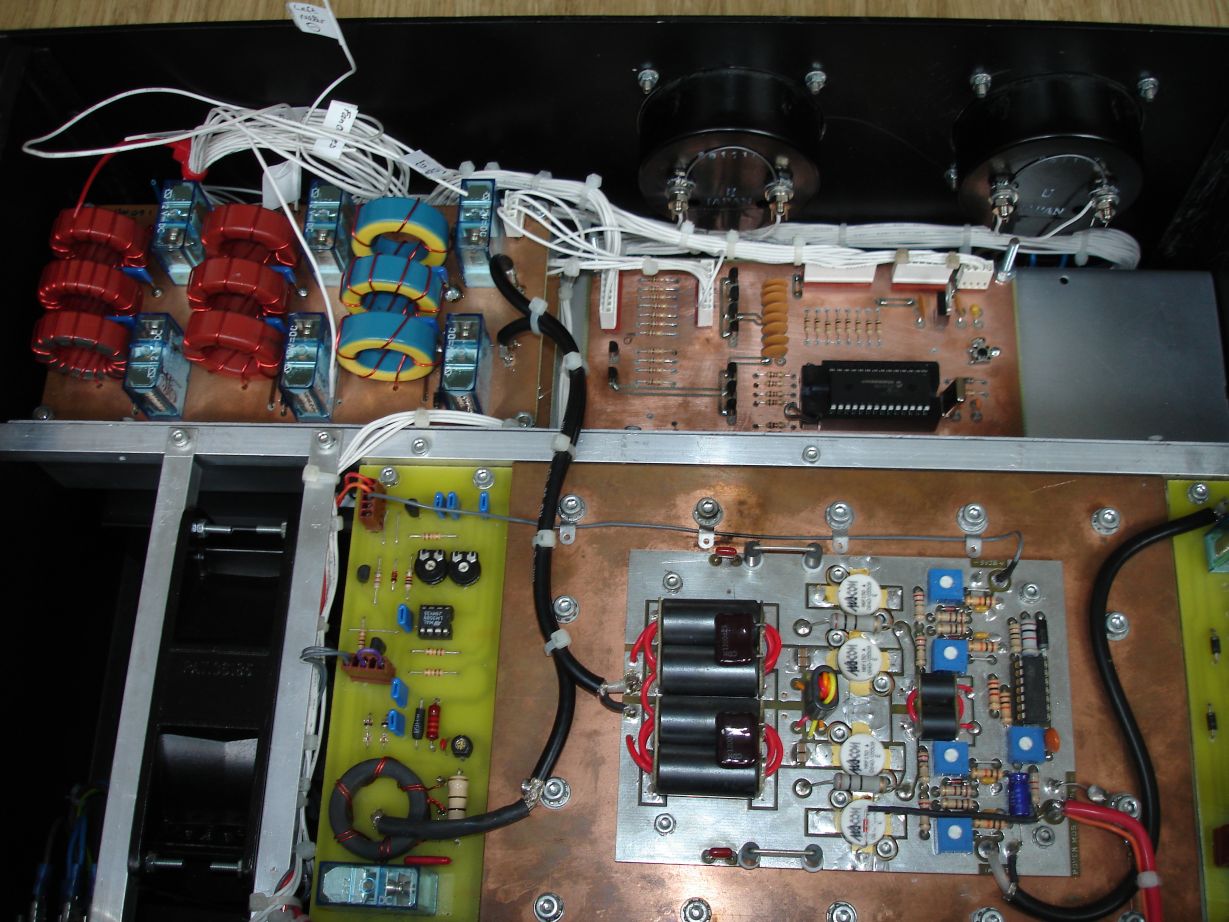
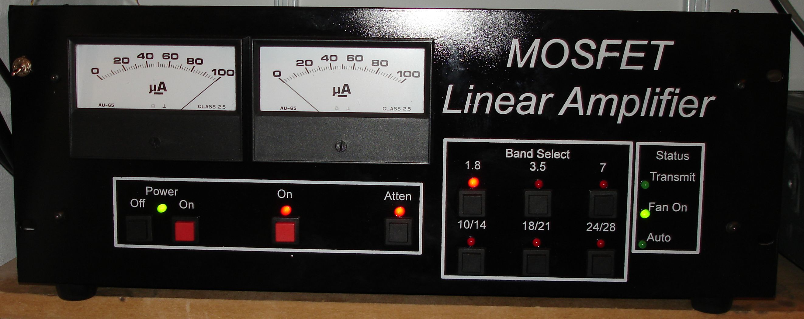
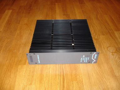
Completed Hardware
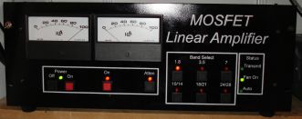
.
Above are pictures of the current hardware which is more less
final - at least until I change it.
Software Updates
21 April 2013
I
have modified the software to ensure if band is changed automatically
then the amplifier is turned off. Otherwise it would be too
easy
to change band on the radio and go to transmit with the amplifier in
but without matching the aerial - not good.
The software will now
work
with any Icom radio not just the IC735.
The IC735 was the first radio to implement the CI-V and used
a 4
byte data string for the frequency rather than 5 used on later models.
The software can now cope with either, I've tested with an
IC706
and it works fine - only after 4 hours of messing about just
to
discover I had to enable the Transceive function on the IC706 for it to
produce data, oh well......
28 April 2013
I recently
bought a Kenwood TS480 which I am really enjoying playing with,
particularly the remote control abilities. Obviously I want
it to
able to control the amplifier so I have been looking at the Kenwood
Network System (KNS). The key document has been this
one. So far
I have gleaned a few things:
- it has a separate txd and
rxd
line (unlike CI-V which has a single line)
- standard RS232C voltage
levels
are used (+15V and -15V)
- it seems to only be
suitable
for one radio controlled by one PC (unlike CI-V which is a CSMA-CD
system)
- to get the rig to output
it's
parameters as they are changed on the front panel (as opposed to
interrogating it for its status) it has to have the Auto Information
set to on. This is done by sending it the command AI2; .
Unfortunately this is
cleared back to off when the rig is powered off.
I sent it a few commands
by hand to check
I understood this. To do this I used the terminal program Tera
Term.
This is very useful for checking things out. I have
reached
a few conclusions based on the above:
- the amplifier cannot just
passively monitor the data coming out from the radio as there won't be
any unless you send AI2; to the radio
- when the amp is turned on
it
will need to send AI2; as part of its start up sequence
- to have PC control of the
radio
via HRD
and
the amp connected, then
the
amp will have to take over the rxd and txd lines to the radio, send
AI2; to the rig, and then connect the lines back to the pc and HRD.
This will probably mean looping the radio to the amp and then
the
amp to the pc
- to ensure when the amp is
off
that HRD will still work then I may have to use relays to switch txd
and rxd
- the current comms board
will
need to be modified to bring out rxd and txd separately, currently they
tied together to drive the CI-V interface - I should have thought about
keeping them separate earlier.....................!
My
current thinking is to have an extra small board on the back of the
radio which feeds two 9 way D types, one from PC, one from radio.
The board will then have some relays for txd and rxd
switching
and some sort of control line to switch it for Icom, Kenwood, or even
Yaesu (if I can be arsed to do it). The only thing that
really
worries me is having to drill the chassis as I will have to do it with
all the electronics in the case. I'll see if I can borrow a 9
way
D type hole punch from work.
Switching
Noise.
The
switched mode 50V psu was causing
some switching noise on some bands, particularly 15m. However
it
does
have a control input
to turn it on, although checking showed the manual to be wrong on the
pin number; it is 12b not 12d. I
am using the input to power it down on receive, and then power up on
transmit. The only slight snag is that it takes a short time
for
the
50V to come up once the control line enables it. I could
measure
how
long it takes but I can't be bothered as there is nothing I can do
about it.
Bugs fixed:
- Output power varies band
to
band - this turned out to be the bias switching transistor not going on
fully. Reducing the base resistor fixed it.
- RF getting into the
processor
making it switch bands etc when on transmit - not good!. The
copper earth plane on top of the board (clearly visible above RF board
in the pic above) was not earthed. Obvious really, but it
took me
a while to find......
Bug
to still fix - RF output
varies band to band.
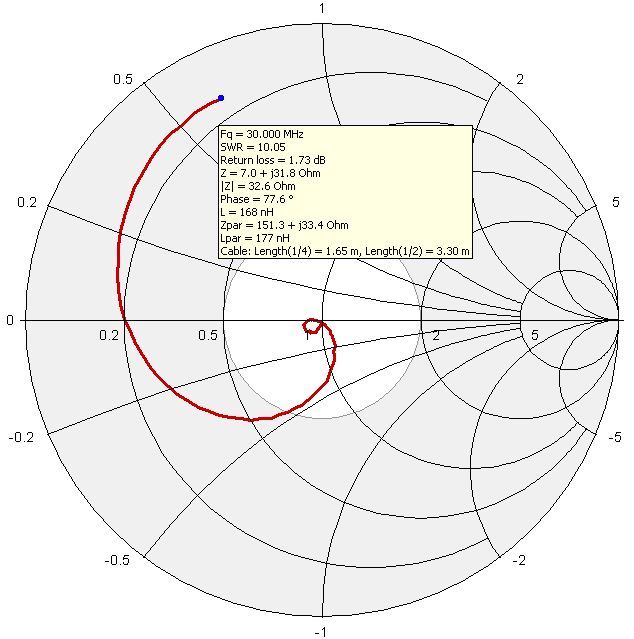
I've yet to figure this one out.
I suspect the filters are maybe presenting a poor match to
the RF
board. I've taken some Smith charts to see if there is a clue
there. Here's some results:
Top band in-band and at second harmonic which looks ok:
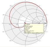

18MHz in-band and at second
harmonic which does not look ok:

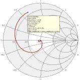
Trouble is, they both seem to work all right so this is still work in
progress..........
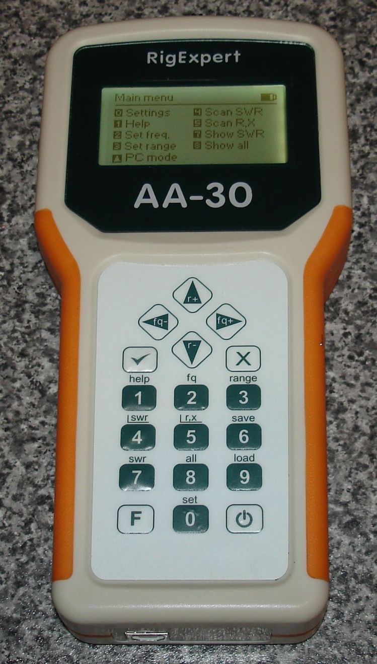
These plots were taken using a RigExpert
AA30

This is overtly an antenna analyser but is much more powerful than that
as it can determine Z, R and X, including the sign of X. Most
analysers don't seem able to do the sign of X. The user and
software
manual tell you more if you are interested.
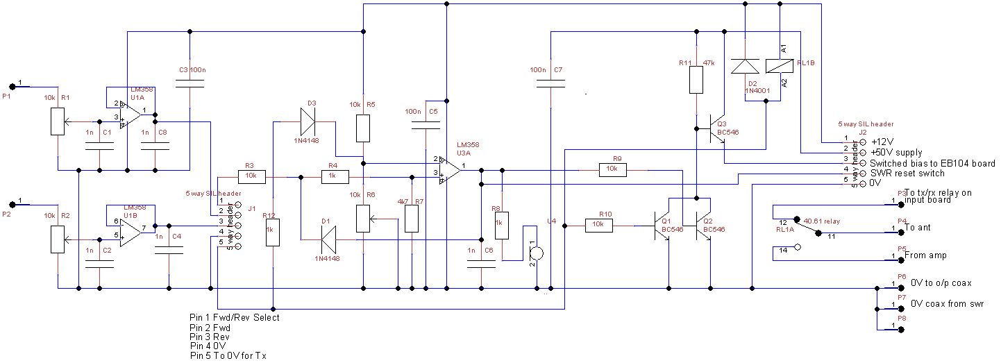
SWR
protection Board
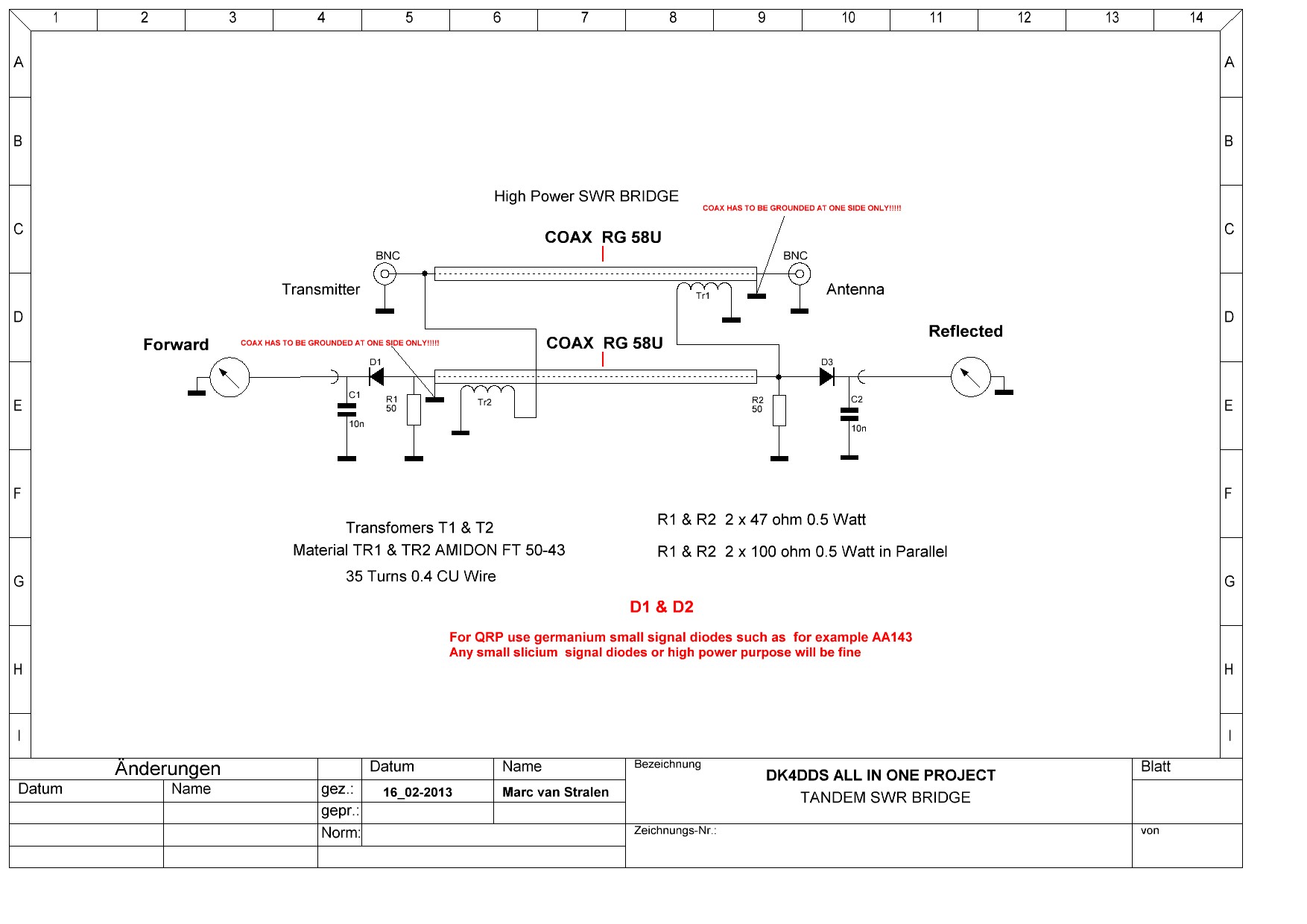
The
original SWR protection board
just did
not work :-( I don't seem able to measure the SWR effectively
so
this board needed a redesign. Marc van Stralen, DK4DDS has
sent
me
some helpful information by Bill Leonard, N0CU. He also gave
me a
link to his All in one SDR TRX.
This is a
great project and includes a high power SWR bridge design which I have
partly replicated.
I have taken the SWR bridge parts and combined them with buffering and
latching circuits to provide protection. Here is Marc's
bridge
design:
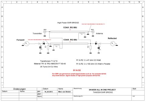
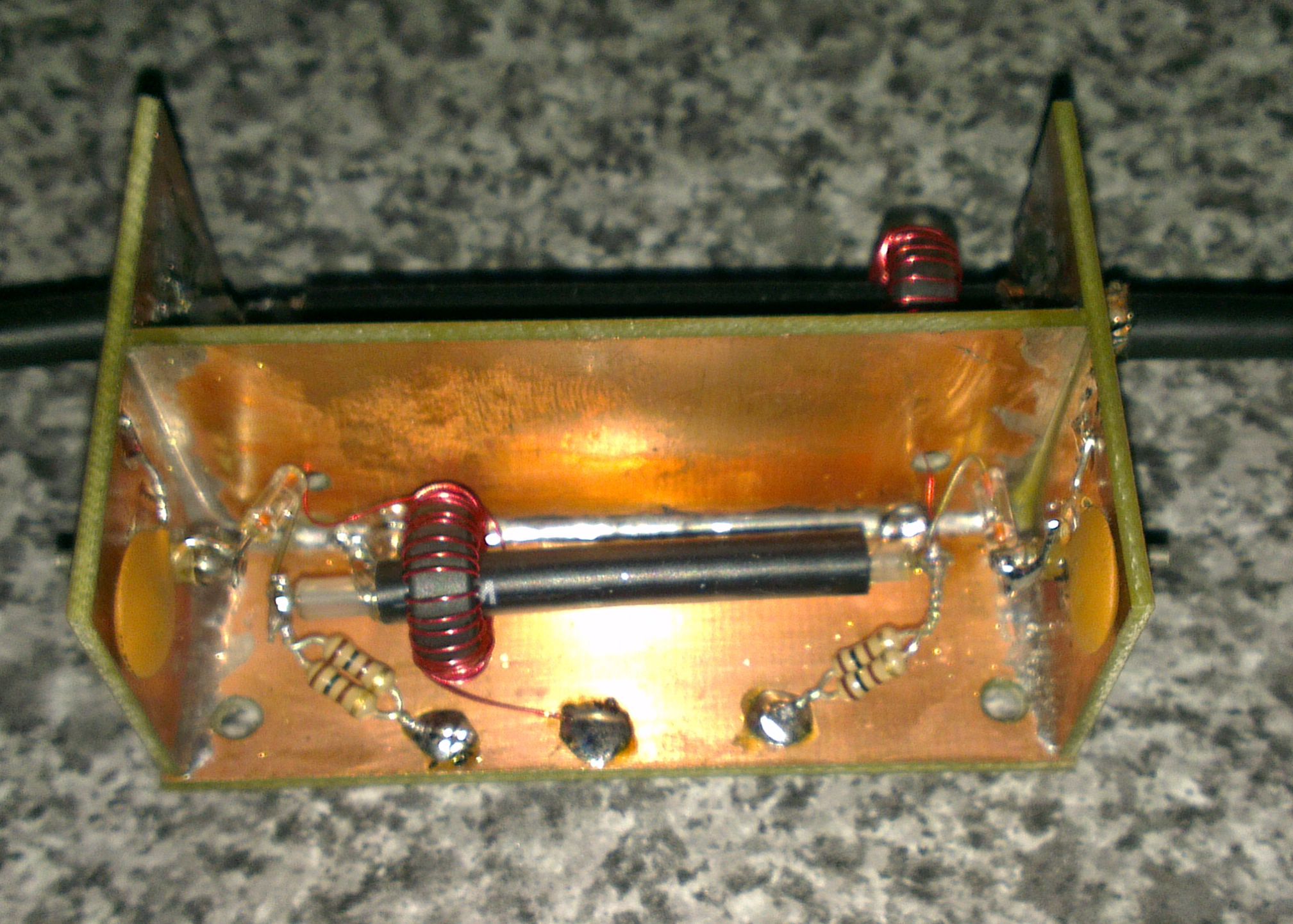
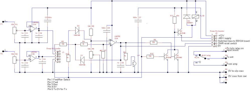
My implementation of this looks like:

The circuit to go with this contains buffers, a latch, a piezo
buffer to warn of excessive SWR plus some 50V bits to remove the bias.
If it works as I hope (!) then putting the amp back to
receive
should reset the latch. I haven't yet built it so we will
see.......
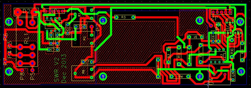
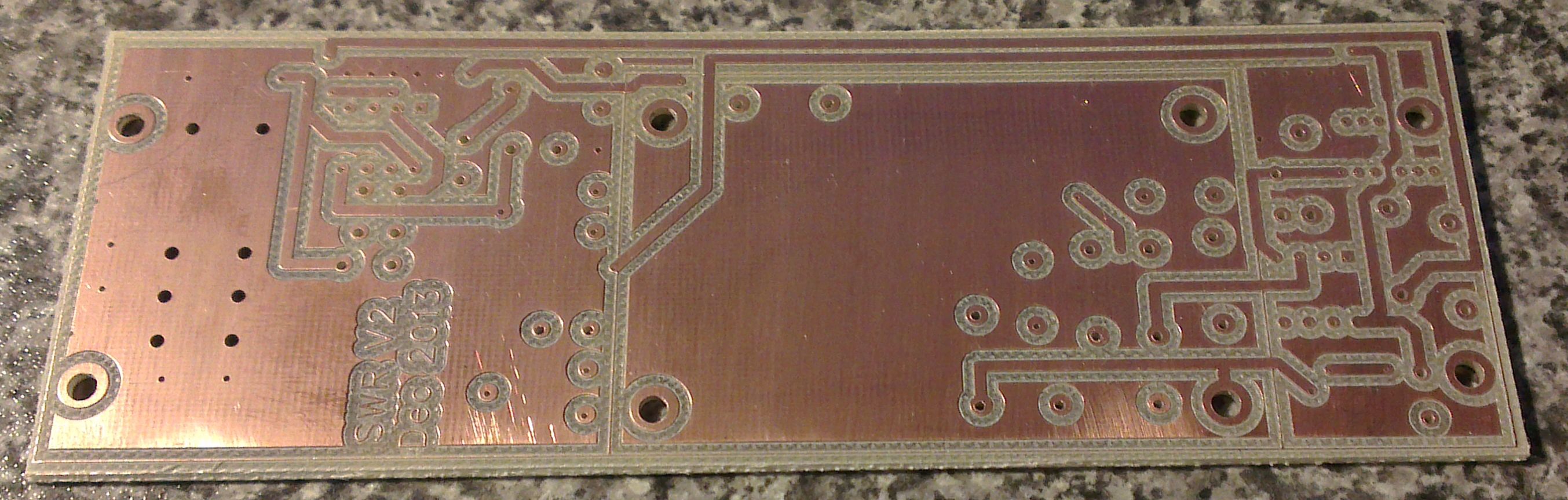
I have designed the PCB for this, the main problem is that the bridge
parts are rather big and so has to sit above the omp amp etc pcb.
The PCB is:
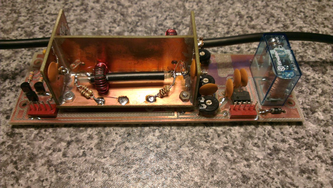
The populated board before fitting into the amp:

This is now fitted into the amp and works as intended. The
only
thing I had to do was to reduce R3 from 10k to 1k as the voltage at pin
3 of U3 was too small. Here it is in situ.
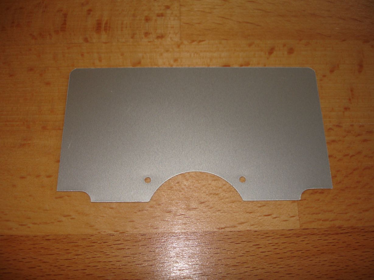
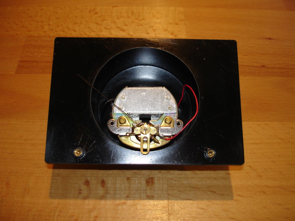
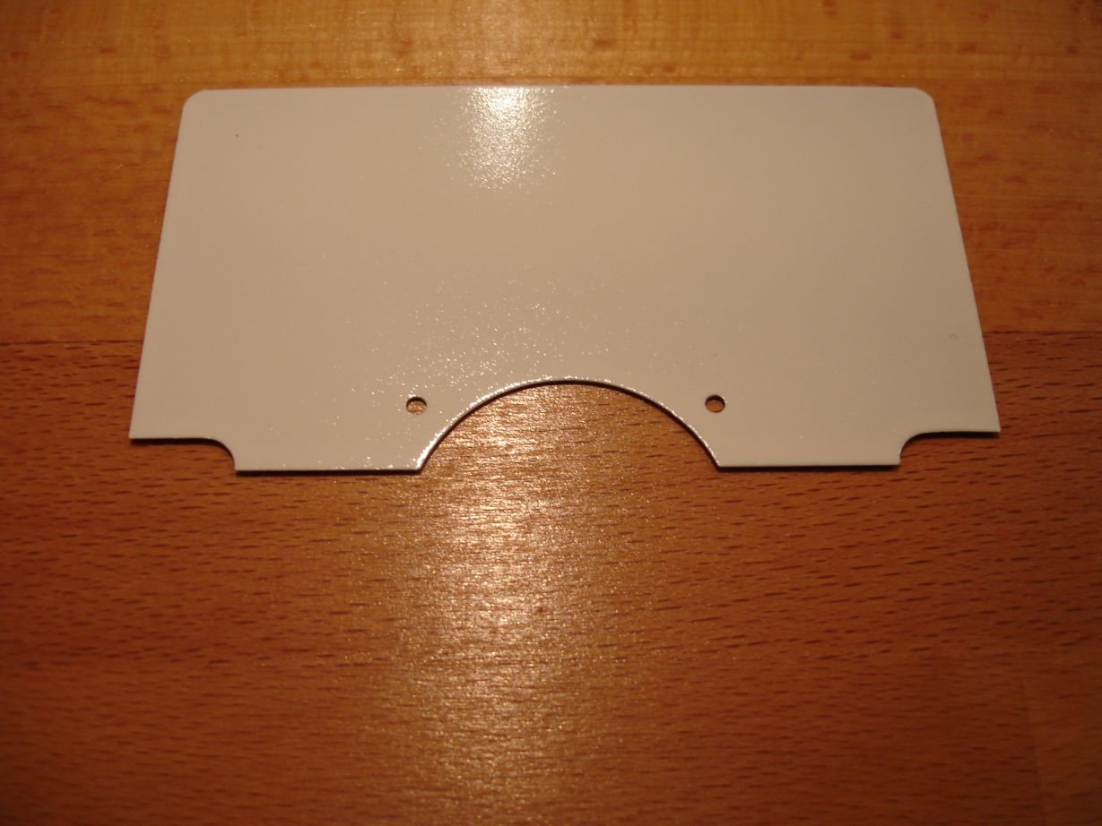
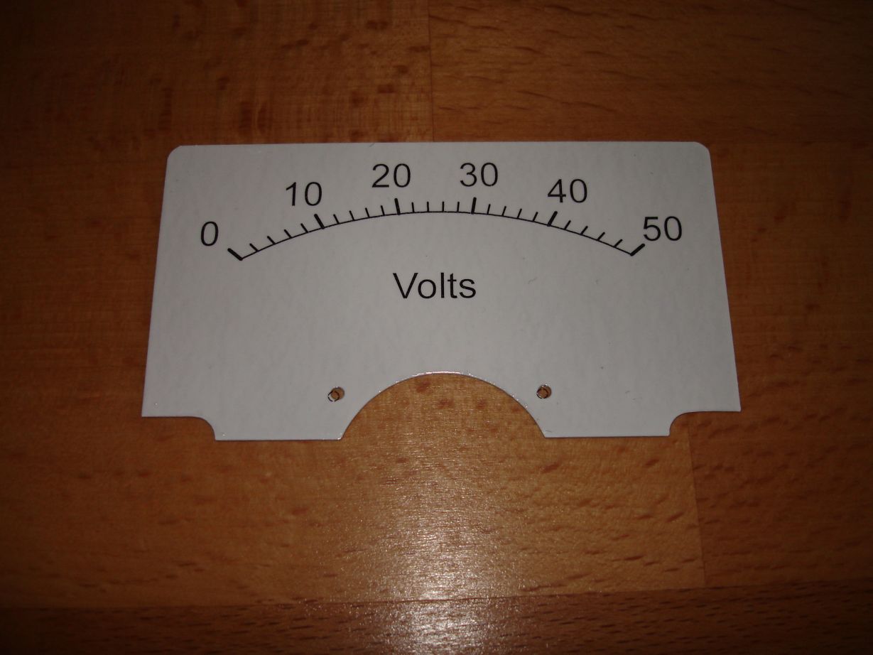
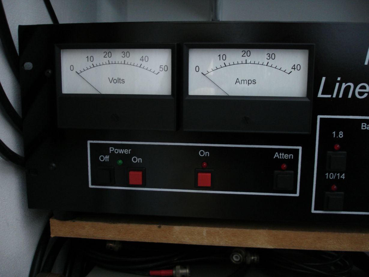
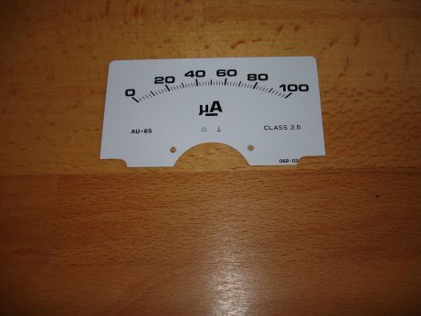
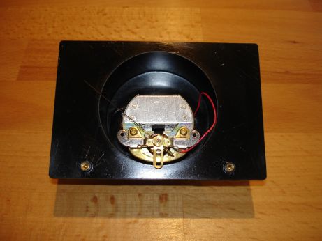
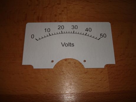
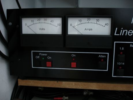
Meter Scales
I bought the meters for the drain current and voltage at a radio
rally (can't remember which or when) and although they are the right
size they obviously have the wrong scales. I did a bit of
Googling and found MeterBasic
at Tonne Software. This was ideal in terms of generating a scale
but the snag was how to get it on to the meters. I eventually
bought some paper intended for generating "decals" on models and
similar. I got this off Amazon from Mr Decal Paper. I
assume you can also get it from them directly.
It was not cheap at about £2 per A4 sheet but looked
suitable. The process was take the meter scales off, flip them
over, paint them white, put on the decal and then seal with a clear
lacquer. The process and outcomes are below, the paints are car
spray paints from Halfords.

Next job is to do a hardware mod and write some more code to allow this
to interface properly to Kenwood radios. There are lots of other
projects to do first though...................
Bob
Harris, G4APV, 3rd September 2014